Introduction
The realization of high conducting p-type GaN film is one of the key factors to the success of GaN based light emitting devices such as light emitting diodes (LEDs) and laser diodes with low series resistance and high external quantum efficiency. Mg has been used as a typical acceptor dopant in GaN grown by metalorganic chemical vapor deposition (MOCVD), known to have the smallest ionization energy compared with other acceptor dopant sources. Nevertheless, it is difficult to get the p-type GaN with low resistivity and high hole concentration because it is still deep from valence band maximum. Recently, it was theoretically suggested that co-doping of n-type dopants (eg. Si, O, etc.) together with p-type dopants (eg. Mg, Be, etc.) in GaN is effective for the fabrication of high-conductivity p-type GaN[Reference Yamamoto and Yoshida1, Reference Brandt, Yang, Kostial and Ploog2]. It drives us to the study of co-doping characteristics in p-type GaN.
In this work, we have studied the co-doping characteristics of Si with Mg as well as Zn with Mg.
Experiments
All samples were prepared in a horizontal MOCVD reactor. The source materials of Ga, N, Mg, Si, and Zn are trimethylgallium (TMGa), ammonia (NH3), bis-cyclopentadienylmagnesium (Cp2Mg), 100 ppm monosilane (SiH4), and diethylzinc (DEZn), respectively. Mg doped, Mg-Si, and Mg-Zn codoped GaN overlayers with thicknesses of 1 – 2 microns were grown in H2 ambient at 1080 °C with various flow rates of Cp2Mg, SiH4, and DEZn. Other growth conditions are the same with those of the unintentionally doped GaN[Reference Kim, Oh, Lee, Yang, Hong, Lim, Yoshikawa and Lee3].
Results and Discussion
Mg doped GaN
In order to investigate Mg doping characteristics in GaN, several kinds of GaN films with different hole concentrations obtained by varying the amount of Cp2Mg flow rate were grown. Figure 1 shows typical Hall characteristics of the GaN films as a function of gas phase [Mg]/[Ga] ratio measured at room temperature after post-growth rapid thermal annealing (RTA) in N2 ambient for 30 s at 900 °C. Electrical characteristics were evaluated using the conventional van der Pauw Hall measurement in which magnetic field of 0.5 Tesla and currents between 10 and 100 uA are applied. The GaN grown under a [Mg]/[Ga] ratio of 5.4 × 10⁻³ gives a high resistivity of 5.6 Ωcm and a low hole concentration of 7.3 × 1016 cm−3. When the [Mg]/[Ga] ratio is reached to 7.6×10⁻³, the hole concentration and resistivity abruptly change and have the maximum value of 6.7×1017 cm−3 and the minimum value of 0.8 cm, respectively. If the [Mg]/[Ga] ratio is larger than 7.6×10⁻³, the hole concentration is gradually decreased and the resestivity is increased.

Figure 1 , Dependence of resistivity (solid circle) and hole concentration (open circle) at room temperature on the gas phase [Mg]/[Ga] ratio during the growth of GaN.

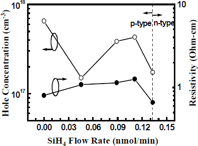
Figure 2 , The resistivities (solid circles) and hole concentrations (open circles) as a function of SiH4 flow rate during the growth under the constant [Mg]/[Ga] ratio of 7.6 ×10⁻³.
Mg-Si co-doped GaN
For the purpose of studying Si co-doping characteristics in Mg doped GaN films, some kinds of specimens with different SiH4 flow rates were grown where the [Mg]/[Ga] ratio was kept constant to 7.6 × 10⁻³ thought to be the optimum condition. The Hall characteristics of the samples as a function of SiH4 flow rate are exhibited in Fig. 2, which are carried out after the identical RTA treatment as mentioned earlier. The Si and Mg co-doped p-type GaN layers show anomalous electrical behaviors. If considering only absolute net acceptor and donor concentrations, one can easily predict that hole concentrations are gradually decreased with increasing SiH4 flow rate, and finally type conversion arises. However, actual experimental data do not follow our expectation. In other words, the hole concentrations are increased as SiH4 flow rates increase before occurring type conversion. It is also interesting fact that type conversion occurs at a SiH4 flow rate of 0.13 nmol/min, because this value is the quantity corresponding to the doping level of 1 × 1017 cm−3 when applied in an undoped GaN. In addition, the maximum hole concentration (4.5 × 1017 cm−3) of p-GaN co-doped with Si and Mg shows the lower value compared to that (6.7 × 1017 cm−3) of only Mg doped GaN. This abnormal behavior could be figured out by introducing the concept of competitive adsorption between Mg and Si atoms because they get into the same Ga sublattice site, though the quantity of Si atom is much less than that of Mg atoms in gas phase. Actually, if we compare the bond length of Si - N and Mg – N, the bond length of Mg – N (0.1439 nm) is shorter than that of Si – N (0.1572 nm)[4]. Since the formation energy of Si – N bonding is smaller than that of Mg – N, the occupation by Si atom into Ga sublattice site is easier than that by Mg atom. Accordingly, for Mg and Si co-doped GaN films, we presume that somewhat larger amount of Si atoms and smaller amount of Mg atoms are introduced into the co-doped GaN film than those independently calibrated. Besides, for [SiH4] < 0.13 nmol/min, it is reasonable that the hole concentration is increased with increasing SiH4 flow rate because the increase of Si donors prevents from generating native defects leading to the self-compensation[Reference Yamamoto and Yoshida1]. Therefore, this assumption can explain the experimental Hall data successfully and be proven by low temperature (100 K) measured PL spectra shown in Fig. 3.
Low temperature (100 K) photoluminescence (PL) spectra of GaN epilayers with different [Mg]/[Ga] ratios are shown in Fig. 3 (a). The peaks at 3.25 eV and 2.77 eV are attributed to donor-acceptor pair (DAP)[Reference Kaufmann, Kunzer, Maier, Obloh, Ramakrishnan, Santic and Schlotter5] and deep donor-acceptor-pair[Reference Viswanath, Shin, Lee, Yu, Kim, Kim, Choi and Hong6] transitions, respectively. However, at present status, we can not explain the exact origins of transition lines peaking at 3.17 eV and 3.01 eV. It is apparent that blue emissions around 2.77 eV are increased and DAP transitions about 3.2 eV are quenched as [Mg]/[Ga] ratio increases. This means that the transition probability from the deep donor state to acceptor level is more probable and intense than that from the shallow donor state because the amount of deep donor is increased as Mg incorporation increases. This result shows good agreement with the electrical characteristics shown in Fig. 1.
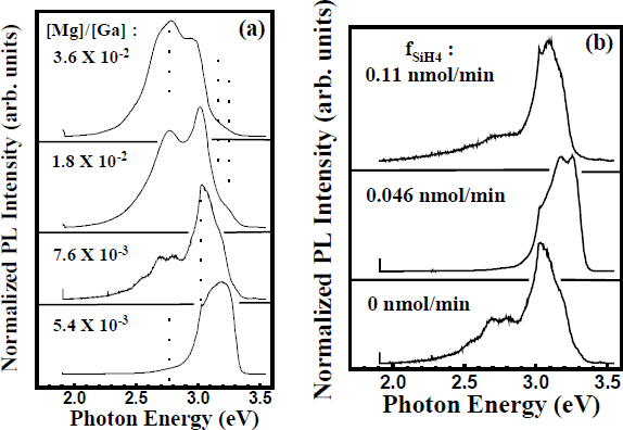
Figure 3 , Low temperature (100 K) measured PL spectra of (a) Mg doped GaN films with various [Mg]/[Ga] ratios, and (b) MgSi co-doped GaN films with different SiH4 flow rates when keeping the [Mg]/[Ga] ratio constant to 7.6 × 10⁻³.
The PL spectrum of Si and Mg co-doped GaN film with the SiH4 flow rate of 0.046 nmol/min in Fig. 3 (b) is similar to the result of the PL spectrum of Mg doped GaN layer with the [Mg]/[Ga] ratio of 5.4 × 10⁻³ as shown in Fig. 3 (a). It means that the introducing SiH4 source reduces the incorporation of Mg atoms, as we suppose.
Mg-Zn co-doped GaN
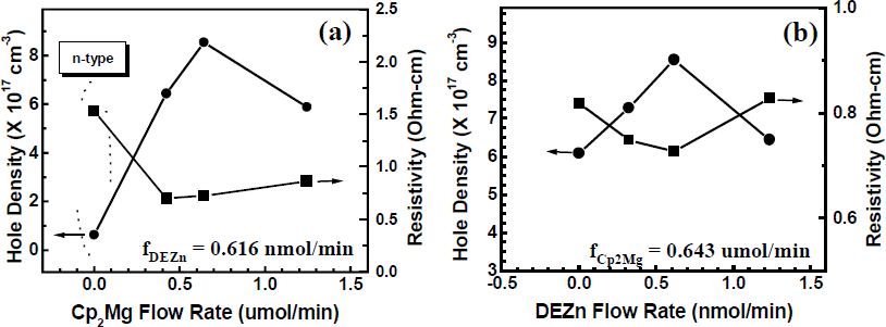
As we change Cp2Mg (under constant DEZn flow rate of 0.616 nmol/min) and DEZn (under constant Cp2Mg flow rate of 0.643 umol/min) flow rates, the variations of hole densities and resistivities of Mg-Zn co-doped GaN films at room temperature are shown in Fig. 4 (a) and (b), respectively. Theoretically, the co-doping of two different p-type dopants in GaN is not helpful to achieve a high conducting p-type GaN, because it forms a lot of native defect levels leading to hole compensation. However, in our prepared samples, we observed there exist optimum Cp2Mg flow rate of 0.643 umol/min and DEZn flow rate of 0.616 nmol/min showing higher hole concentration (8.5 × 1017 cm−3) and lower resistivity (0.72 Ωcm) than those for only Mg-doped GaN film.

Figure 4 , Dependence of hole densities and resistivities for the Mg-Zn co-doped GaN films at the condition of (a) various Cp2Mg flow rate and constant DEZn flow rate of 0.616 nmol/min , and (b) various DEZn flow rate and a constant Cp2Mg flow rate of 0.643 umol/min.
Besides, from the high resolution x-ray diffraction (HRXRD) measurement as shown in Fig. 5, both (002) and (102) HRXRD full width at half maximum values are broadened by increasing Cp2Mg flow rates not DEZn flow rates. So we can conclude that the incorporation of Zn atoms with Mg is the technique obtaining high conducting p-type GaN film without deterioration of the structural qualities of GaN films.
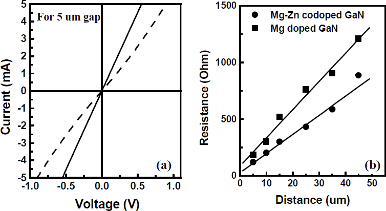
In order to compare Ohmic contact properties for the only Mg-doped (6.0 × 1017 cm−3) and the Mg-Zn co-doped (8.5 × 1017 cm−3) p-GaN films, we performed transmission line method (TLM) with ring contact geometry with outer ring radius of 200 um and gap spacings (5 – 45 um). The surface of p-type GaN specimens were treated using aqua regia[Reference Kim, Lee, Lee, Shin, Park and Kim7], followed by the deposition of Pd(150 A)/Au(1400 A) Ohmic metals under a vacuum condition of 10−5 torr. After the metal deposition, the photoresist was lifted off. Current-Voltage (I-V) characteristics of the prepared samples were measured by HP 4155 parameter analyzer.

Figure 5 , Dependence of (002) and (102) HRXRD FWHMs for the Mg-Zn co-doped GaN films at the condition of (a) various Cp2Mg flow rate and constant DEZn flow rate of 0.616 nmol/min , and (b) various DEZn flow rate and a constant Cp2Mg flow rate of 0.643 umol/min.

Figure 6 , (a) Comparison of the I-V characteristics measured between the contact pads with a gap spacing of 5 um. for the only Mg-doped (dashed line) and Mg-Zn co-doped p-type GaN films(solid line), (b) Variation of resistance as a function of gap spacing for the only Mg-doped (Solid square) and Mg-Zn co-doped (solid circle) p-type GaN films. solid lines are linear fits of experimental data.
Figure 6 (a) shows the I-V characteristics for both the only Mg-doped and the Mg-Zn co-doped GaN samples, measured between the Ohmic pads with a spacing of 5 um. The I-V curve obtained is nonlinear for the only Mg-doped sample, but linear for the Mg-Zn co-doped sample over the whole range of voltages. The specific contact resistivities with correction factors [Reference Lester, Brown, Ramer, Zhang, Hersee and Zolper8] taken from the gradients and intercepts in the Fig. 6 (b) are determined [Reference Lester, Brown, Ramer, Zhang, Hersee and Zolper8] to be 1.9 × 10⁻³ Ω cm2 for the only Mg-doped sample and 5.0 × 10⁻⁴ Ω cm2 for the Mg-Zn co-doped sample. Note that contact resistivity decreases by one order of magnitude by the co-doping technique. Therefore, the Mg-Zn co-doped GaN layer is expected to act as a good contact layer in device structure.
Summary
We have found that Mg doped GaN layer shows high electrical conductivity, when the [Mg]/[Ga] ratio in gas phase is 7.6 × 10⁻³. The Mg-Si co-doping characteristics were explained effectively taking advantage of the concept of competitive adsorption between Mg and Si during the growth. In other words, the occupation by Si atom into Ga sublattice site is easier than that by Mg atom, since the formation energy of Si – N bonding is smaller than that of Mg – N. We have also grown p-GaN film with a resistivity of 1.26 Ωcm and a hole density of 4.3 × 1017 cm−3 by means of Mg-Si co-doping technique. For Mg-Zn co-doping, p-GaN showing low electrical resistivity (0.7 Ωcm) and high hole concentration (8.5 × 1017 cm−3) was successfully grown without the degradation of structural quality of the film. Besides, the specific contact resistance for Mg-Zn co-doped GaN film measured by TLM is 5.0 × 10⁻⁴ Ωcm2, which is lower value by one order of magnitude than that for only Mg-doped GaN film (1.9 × 10⁻³ Ωcm2).
Acknowledgements
This work has been supported by the KOSEF and the MOST of Korea through the Semiconductor Physics Research Center at Chonbuk National University.