


I. INTRODUCTION
The integration of coherently strained epitaxial quantum dots (QDs) into semiconductor devices requires size and position control for device functionality. Surface templating to direct self-assembly of the site-controlled QD arrays can provide precise positioning and improved size homogeneity versus randomly nucleated QDs. Reference Zhong and Bauer1 Additional benefits to patterning include the potential to increase the areal density of QDs, the use of the 2D ordered QD array as a “seed layer” to create 3D ordered QD arrays, Reference Grützmacher, Fromherz, Dais, Stangl, Müller, Ekinci, Solak, Sigg, Lechner, Wintersberger, Birner, Holy' and Bauer2 and ultimately the exploitation of interdot electronic interactions to create materials with novel, precisely tailored properties. Reference Pryor, Flatté and Levy3,Reference Fromherz, Stangl, Lechner, Wintersberger, Bauer, Holy, Dais, Müller, Sigg, Solak and Grützmacher4 Various surface features have been used to direct QD nucleation including pits, Reference Zhong, Halilovic, Mühlberger, Schäffler and Bauer5–Reference Karmous, Cuenat, Ronda, Berbezier, Atha and Hull7 stripes, Reference Zhong, Halilovic, Mühlberger, Schäffler and Bauer5,Reference Kamins and Williams8 mesas, Reference Kitajima, Liu and Leone9,Reference Jin, Liu, Thomas, Luo, Wang and Nguyen10 and oxide windows, Reference Yoon, Kim, Kim, Ryu, Russell, Zhao, Liu and Xie11 which are formed via techniques including lithography, nanoindentation, and ion-beam processing. The reported growth experiments cover a wide range of pattern densities, growth temperatures, and areal coverage, yielding highly uniform arrays of ordered QDs. For the Ge/Si (001) heteroepitaxial system, pattern spacings (pitches) are typically in the range of 100–500 nm, corresponding to areal densities of 4 × 10⁸ to 1 × 1010 cm−2. In this work, we routinely attain 50 nm interdot pitch (center-to-center site spacing), resulting in well-ordered arrays of Ge QDs with reasonably narrow size distribution. Preliminary QD patterns at 35 nm pitch were attained, but with reduced homogeneity. The challenges to directed self-assembly, associated with both initial pattern uniformity and Ostwald ripening of QDs, become severe as the length scales are reduced toward 10 nm, where confinement and exchange coupling between QDs could provide interesting and useful tailoring of the electronic structure. Reference Katsaros, Spathis, Stoffel, Fournel, Mongillo, Bouchiat, Lefloch, Rastelli, Schmidt and DeFrancheschi12–Reference Fiedler and Kratzer17
Heteroepitaxial Ge islands form to partially relax the 4% lattice mismatch strain with the Si substrate. QD formation requires growth conditions where adatom diffusion lengths match or exceed the intrinsic length scale, λ ≈ Δγ/Mε2, where Δγ is the surface energy change when QDs form, and Mε2 is the elastic energy density in the Ge due to the lattice mismatch. Reference Srolovitz18 At the growth temperatures used here, after the formation of a 3–4 monolayer (ML) thick planar wetting layer, pyramidal Ge QDs form on a planar substrate, followed by the so-called dome clusters. Reference Medeiros-Ribeiro, Bratkovski, Kamins, Ohlberg and Williams19 At significantly higher temperatures, domes may actually form first. Reference Brehm, Montalenti, Grydlik, Vastola, Lichtenberger, Hrauda, Beck, Fromherz, Schäffler, Miglio and Bauer20 Surface templating ostensibly creates a locally varying chemical potential through modification of the surface curvature (or step density), surface strain, and/or surface chemistry. Reference Yang, Liu and Lagally21 A large body of work specifically examines the effects of the changing surface morphology on the preferred nucleation of Ge QDs. However, the actual siting of the dots, e.g., inside or outside of pits, on top or on bottom of ridges, is surprisingly variable. While some clarity is beginning to emerge, it is clear that much remains to be understood, especially when the pattern pitch approaches, or is smaller than, the QD intrinsic length scale, λ.
Here we employ a Ga+ focused ion beam (FIB) and defect-selective wet chemical etching to create a continuously height-modulated (quasi-sinusoidal) surface, rather than the discrete pits or ridges used in the existing literature. This modulated surface has a profound effect on QD nucleation. FIBs have been used earlier to template Ge QDs Reference Karmous, Cuenat, Ronda, Berbezier, Atha and Hull7 as well as other Ge nanostructures. Reference Hull, Floro, Graham, Gray, Gherasimova, Portavoce and Ross22 They possess unique advantages compared to photolithographic techniques including the direct writing of patterns, i.e., resist or pattern transfer are not required, and the ability to rapidly write complex, asymmetric patterns without the need for a mask. High-fidelity pattern replication has been reported for Ge QDs grown on FIB-patterned surfaces, although loss of fidelity was reported below 100 nm pitch due in part to competition between adjacent sites. Reference Gherasimova, Hull, Reuter and Ross23
We use an ultra-low-dose FIB to pattern Si(001), and relatively low growth temperatures (450–550 °C), to obtain Ge QD arrays with high areal density, 4 × 10¹⁰ dots/cm2, and low site vacancy fractions. There is a correlation between QD growth fidelity and pattern dose, which is also sensitive to the growth temperature. Unlike previous reports, our QDs do not nucleate within the pits, but in the 4-fold regions between the pits, referred to here as “crowns”. Due to the high density of the patterns, the interpit regions are not (001) terraces, but have nonzero curvature. These crowns act as preferred nucleation sites. Potential mechanisms are discussed in the context of existing results and theories.
II. EXPERIMENT
Si (001) wafers with <0.1° miscut were cleaned with a 4:1 H2SO4:H2O2 solution, stripped in 5% HF, and passivated in UV ozone prior to loading in a FEI Helios Nanolab 650 Ga+ FIB system. The wafers were oxygen plasma cleaned in situ prior to patterning. The FIB was operated with an accelerating voltage of 30 kV and emission current of 1.1 pA with a manufacture specified beam diameter of 7 nm. To ensure a circularly focused beam, the beam was focused and destigmatized at a magnification of 150 kx. The beam circularity was checked by imaging a reference pattern in a scanning electron microscope (SEM) mode. All patterns for this work consist of FIB-illuminated sites on a square lattice. Within a 100 μm × 100 μm field we wrote an array of patterns of various doses ranging from 700–69 K ions/site and lattice spacings typically 50, 35, and 20 nm. The individual patterns contain as many as 500 K sites.
The patterned wafers were cleaned again with a modified IMEC/Shiraki process Reference Kassim, Nolph, Jamet, Reinke and Floro24 and then stripped in a 5% HF solution prior to loading into an ultra-high vacuum (UHV) molecular beam epitaxy (MBE) chamber (P base = 1 × 10⁻¹⁰ Torr). In the MBE chamber the sample was radiatively heated to 280 °C for 30 min to degas. The sample was further heated to 550 °C (33 °C/min) for 5 min to desorb H. The surface structure was monitored with reflection high-energy electron diffraction throughout the process. The substrate temperature was then reduced to 450 °C (500, 550, and 625 °C in subsequent growths). Ge of 5 ML thickness was deposited via magnetron sputtering in 5 mTorr of getter- and LN2-purified Ar at a rate of 0.11 Å/s directly on the pattern without any Si buffer layer.
To directly compare the resulting Ge QD formation and the underlying surface pattern, the QDs were first characterized by atomic force microscopy (AFM). For the sample grown at 450 °C, the Ge was then selectively etched by submerging the wafer in 65 °C deionized water for 2 h, dried by dry N2, and then rescanned by AFM. The AFM was performed with a NT-MDT Solver Pro-M in semicontact mode using NSG01/NSG10 tips with a typical radius of 6 nm. The sample patterns were intentionally misaligned relative to the AFM scan direction to reduce flattening artifacts between the QDs. Select specimens were also examined using SEM.
III. RESULTS
AFM images of the as-written FIB patterns reveals net sputtering, i.e., direct formation of a milled pit, only at doses of 69 K ions/site and above, as shown in Fig. 1(a), whereas at 34 K ions/site and below, raised surface features are present at the FIB-implanted sites, Fig. 1(b). This arises from the defect generation and Ga+ implantation during patterning and subsequent oxidation of the affected regions. Reference Graham, Kell, Floro and Hull25 However, after wet chemical cleaning in preparation for MBE growth, the defective FIB sites are selectively etched, leading to the formation of nanoscale pits, see Fig. 1(c). The final depth and shape of the pit is in part determined by the number of oxidation/stripping iterations.

FIG. 1. AFM micrographs of Si substrate surface after FIB exposure to (a) 69 K ions/site and (b) 34 K ions/site. (c) The surface of the sample in (b) after chemical etching. (d) Lateral line scans of the respective surface topographies (nm). The scans are offset for clarity.
The Ge MBE growth on the FIB patterns resulted in ordered QD arrays that reproduce the desired pattern to varying degrees. Figure 2 shows the AFM micrographs of the patterned Ge QDs with a 50 nm pitch. A select range of ion doses is shown wherein an optimal dose can be identified that produces the best apparent pattern fidelity. “Pattern fidelity” comprises three aspects: (i) location of the QD centroids with respect to the desired 2D lattice, (ii) the volume distribution of the QDs, which ideally would be a delta function, and (iii) site errors, including vacant sites and multiply populated sites. Each micrograph in Fig. 2 only covers a fraction of the patterned area, but the results are typical for the pattern as a whole. To provide a perspective, portions of a larger area scan are shown in Fig. 3; the extended ordering is evident. Long linear features are observed along the array axes 3(b), which are <110>. These lines, where QDs are taller than their surroundings, have the topographical appearance of enhanced growth above misfit dislocations, which would be surprising however, given the small Ge thickness and height-modulated interface.

FIG. 2. 1 × 1 μm AFM micrographs showing the Ge QD morphology on patterns formed with Ga+ doses of (a) 6900 ions/site, (b) 3400 ions/site, (c) 2100 ions/site, (d) 1400 ions/site, (e) 700 ions site, and (f) no pattern. All samples were from a single Ge growth at 450 °C.

FIG. 3. (a) 100 × 100 μm AFM scan showing a typical array of patterns with varying pitch and dose. (b) 10 × 10 μm AFM scan from a 35 × 35 μm array of Ge QDs on a pattern formed using 700 ions/site; (c) shows a higher resolution, 2 × 2 μm, scan from the same large area.
The distribution of QD volumes, sizes (both lateral and vertical), and mean positions of the QDs were determined from the AFM data using analysis techniques built into the software package, Gwyddion. Reference Necas and Klapetek26 The primary concern in determining the QD volume and size is the consistent choice of a threshold value representing the baseline height of the QDs. This analysis was performed on 1 × 1 μm AFM scans (≈400 QDs), which were plane flattened and subjected to a band-pass filter to reduce high-frequency noise and low-frequency baseline variations. The threshold level was varied manually until just before the point when the QD base regions began to merge and percolate with their neighbors. The volumes and sizes are then calculated from this baseline. This will be an overestimate, especially of the volume, due to two effects: (i) tip convolution, which is significant on these length scales, and (ii) incorporation of some contribution from the substrate pattern itself. Regarding tip convolution, Fig. 4 compares the SEM and AFM micrographs from the same Ge QD pattern, where the lateral size of the QDs appears to be about half that obtained by AFM. Of course, the origin of contrast in secondary electron mode of the SEM will determine the apparent QD size; the actual QD diameter lies between the AFM and SEM values. Figure 5 shows the normalized QD volume distribution compared to the normalized crown volume. A key figure of merit included in the table is the scaled width of the distribution, defined here as σs = s/<V>, where s is the standard deviation of the distribution, and <V> is the mean volume. Figure 6 plots <V>, σs, and F m (the fraction of sites missing a QD) as a function of the ion dose. The doses of 3400, 2100, and 1400 ions/site all yield similar results, with the best characteristics at 3400 ions/site, whereas at the 6900 ions/site, the QD pattern was so poor that statistical analysis was not attempted.

FIG. 4. Comparison of apparent QD lateral size in identical areas using (a) AFM and (b) SEM.

FIG. 5. Distributions of QD volumes, and the crown volumes, from the pattern after Ge was selectively removed. Data were obtained from 1 × 1 μm AFM scans on arrays patterned with (a) 3400 ions/site, (b) 2100 ions/site, (c) 1400 ions/site, and (d) 700 ions site. Both the histograms, a Gaussian fit for the QDs (red/solid), and crowns (black/dotted) are shown in each case.

FIG. 6. Ion dose dependence of (a) mean feature volumes (QDs, circles, crowns, triangles) versus ion dose/site, (b) scaled distribution widths (QDs–circles and crowns–triangles) and (c) the QD site error fractions.
Pattern fidelity is also characterized by analyzing the 2D power spectral density function (PSDF), although this convolves both the positional accuracy and the size inhomogeneity. Peaks corresponding to the interdot distance are measured in reciprocal space and transformed to determine the nominal distance between the dots. The full width at half maximum (FWHM) of each is measured to get a sense of variation. The sources of error include miswriting of the array, random centering within each site, as well as the AFM drift. The mean interdot spacing is 52.4 nm with a standard deviation of 1.2 nm and an average FWHM of 4.7 nm.
We examined the effect of the growth temperatures on the QD pattern characteristics in four separate growths. As shown in Fig. 7, an improvement in pattern fidelity is observed at 500 °C. However, at 550 and 625 °C, we observe the onset of coarsening and uniaxial coalescence of dots with clear broadening in volume distribution. Also, coarsening of the on-pattern arrays is clearly suppressed compared to those of the off-pattern QDs.

FIG. 7. 1 × 1 μm AFM micrographs of Ge QDs grown on patterns with 2100 ions/site dose (left column) and corresponding off-pattern QDs (right column) at (a)/(b) 450 °C, (c)/(d) 500 °C, (e)/(f) 550 °C, and (g)/(h) 625 °C.
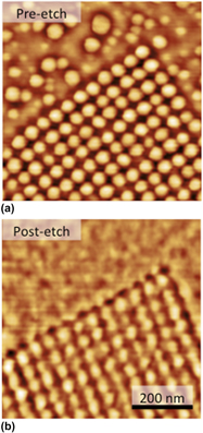
Figure 8 shows the morphology of the underlying Si surface after the Ge is selectively etched away. This allows direct correlation of the resultant QDs with the characteristics of the underlying substrate pattern that was present immediately prior to the growth. By examining the corner regions of each pattern (Fig. 9), we determine that QDs preferentially form in the interstitial locations of the pit lattice (a four-coordinated site), i.e., in the crown, or “on-top” positions of the pattern rather than on the on-bottom positions. This is in strong contrast to the previous reports on directed self-assembly of Ge using pit patterns where the formation occurs preferentially within the pits. Reference Gherasimova, Hull, Reuter and Ross23,Reference Portavoce, Kammler, Hull, Reuter and Ross27–Reference Vastola, Grydlik, Brehm, Fromherz, Bauer, Boioli, Miglio and Montalenti30

FIG. 8. AFM micrographs of the patterned Si surface upon which Ge QDs were grown at 450 °C. Images were obtained by selectively etching off the Ge. (a) 3400 ions/site, (b) 2100 ions/site, (c) 1400 ions/site, and (d) 700 ions site.

FIG. 9. 1 × 1 μm AFM micrographs of a corner of a pattern dosed at 3400 ions/site, (a) 5 ML of Ge at 450 °C, and (b) the same corner after Ge etch.
Furthermore, we find that the patterns where optimal QD formation occurs are not in fact composed of isolated pits in the flat (001) terrace; rather, the surface appears to be continuously height modulated with no flat terrace regions between the pits. The striking resemblance between the before/after micrographs raises the question of whether Ge QDs are self-assembling, or instead, Ge just conformally coats the patterned Si surface. Figure 10 shows the AFM line scans from the micrographs in Fig. 8, overlaying typical scans from similar regions of the patterns. It is clearly seen that net Ge accumulation occurs to form QDs, with a large increase in height from 1–2 nm to 8–10 nm. The local surface angle increases from maximum angles in the Si patterns of about 8°, to up to 30° for the Ge QDs. For the lowest dose examined, 700 ions/site, AFM does reveal that isolated pits separated by (001) terraces are formed, as shown in Fig. 10(d). However, the alignment and ordering of the QDs is actually rather poor in this pattern.

FIG. 10. AFM line scans comparing QDs (gray) to underlying substrate (dashed); all units are in nm. (a) 3400 ions/site, (b) 2100 ions/site, (c) 1400 ions/site, and (d) 700 ions site.
A quantitative analysis was also performed for the patterned Si surfaces after selective removal of the Ge. The scan data are from 1 × 1 μm regions in the center of each pattern. The surfaces were thresholded to measure the volumes of the crowns, as summarized in Fig. 6. The crown periodicity was measured from the PSDF to have an overall average mean spacing of 50.00 nm and a standard deviation of 2.35 nm. We examined the normalized volumetric distributions of both the crowns and their QD counterparts. The QD mean volumes track the crown volumes closely, suggesting that the diffusion between crown sites is highly constrained. While the normalized volumetric distribution width for the crowns monotonically narrows with increasing dose up to 3400 ions/site, the QD volumetric distribution width appears to saturate at σs ∼0.30. There is, however, a continued improvement in the pattern fidelity (i.e., decrease in site errors) along with the decrease in crown volume distribution width up to 3400 ions/site.
IV. DISCUSSION
Many studies have shown that patterned arrays of isolated pits in the Si (001) surface effectively control the nucleation of Ge QDs. An overview can be found in Ref. Reference Grydlik, Langer, Fromherz, Schäffler and Brehm29 by Grydlik et al. and references therein. They show that the patterned pits can act as perfect sinks to form spatially ordered arrays of highly monodisperse Ge QDs (actually alloyed GeSi due to the intermixing during growth) as long as the Ge thickness is carefully limited, and the temperature and deposition rate are controlled so that adatom diffusion lengths match or exceed the pitch. This remarkable work has explored pitches from 300 nm to 3.4 μm and has typically used growth temperatures well in excess of 600 °C, and deposition rates of the order of 0.05 Å/s. These conditions provide diffusion lengths of order 10 μm, but also lead to extensive alloying of the QDs with the substrate. Grydlik et al. have identified at least 10 parameters that strongly affect the site-controlled QD growth during heteroepitaxy. Clearly, the feature sizes of the pattern, which can manifest as the pitch of a periodic pattern, the terrace size, pit size, the spectrum of surface angles etc., are critical parameters, especially in comparison to the intrinsic QD length scale and faceting.
Another key finding (see Vastola et al. Reference Vastola, Grydlik, Brehm, Fromherz, Bauer, Boioli, Miglio and Montalenti30 ) is that the pit sidewall angle has an optimal range of 5–18° for symmetric QD formation at the pit bottom. Above about 32°, the QDs nucleated on the terraces at the edges of the pits (the pit angle here is actually the sidewall angle after Ge-wetting layer growth, which has a somewhat complex interplay with the size of the initial pit, the pit spacing, and the Ge coverage). Using finite element analysis of the elastic energy dependence on the pit angle, Vastola et al., achieved good agreement with the experimental results. This work demonstrates that under conditions where adatom mobility is not limiting, excessively shallow pits do not promote QD formation, intermediate angles lead to QD nucleation in the pit, while sufficiently steep pits lead to QD formation on the (001) terrace region immediately adjacent to the pit.
The pit-patterning approach has been extended to pitches at least as small as 90 nm. The patterns were formed using extreme ultraviolet interference lithography, leading to pits only about 12 nm across and 3–4 nm deep. Reference Grützmacher, Dais, Zhang, Müller and Solak28 In this work, Ge was grown at 450 °C onto 50 nm Si buffers grown at 300 °C. The resultant {105}-faceted pyramidal dots were about 45 nm in lateral size, i.e., the QDs were larger than the pits they nucleated upon Reference Grützmacher, Fromherz, Dais, Stangl, Müller, Ekinci, Solak, Sigg, Lechner, Wintersberger, Birner, Holy' and Bauer2 ; highly monodisperse arrays still resulted, and these were subsequently used to create ordered three-dimensional arrays of QDs.
Portavoce et al. used the Ga+ FIB patterning of Si in a UHV chamber attached to a transmission electron microscope (TEM). Reference Portavoce, Kammler, Hull, Reuter and Ross27 The growth of Ge QDs in the TEM was accomplished using chemical vapor deposition at 550 °C. For optimal patterning dose and postannealing conditions, small Ge QDs ≈ 20 nm in diameter are obtained, on ultrasmall pits found (by ex situ AFM) to be only 10 nm in diameter, 1 nm deep, and 200 nm apart. This work also showed that nanoscale topography, rather than chemical effects from local Ga incorporation, directed the self-assembly.
Pascale et al. used ex situ Ga+ FIB patterning coupled with subsequent MBE growth. Reference Pascale, Berbezier, Ronda and Kelires31 The resulting surface after the buffer growth resulted in discrete pits surrounded by flat (001) terraces, although the size and shape of the pits are not further elucidated. For a 150 nm pitch, growth at 750 °C resulted in QDs forming in the 4-fold crowns (similar to what we observe); however, less than 25% of these sites were occupied. For growth at 550 °C, QDs formed in the pits only, with a high occupation fraction. Based on the observed temperature dependence, and Monte Carlo modeling, they argued that the crown site has a lower total energy than the pit sidewall. However, their model does not actually consider QD formation in the pit bottom.
Using lithographic techniques, Chen et al. etched both pit and hill features into a Si (001) substrate. Reference Chen, Vastola, Lichtenberger, Pachinger, Bauer, Jantsch, Schäffler and Miglio32 To a certain extent, the hill patterns resemble our patterned surfaces, albeit with larger pitches of 200–800 nm, onto which 5 ML of Ge was grown. Highly uniform, dome-shaped islands were observed, located in the saddle points between adjacent hills, as opposed to the four-coordinated minimum between adjacent hills (as seen here). However, the latter location is not actually a true pit, but an intersection between two orthogonal V-grooves. Nucleation on the crowns was not observed.
We have obtained highly dense, ordered arrays of Ge QDs on Si (001) surface-morphological patterns formed using low-dose FIB milling in conjunction with defect-selective etching. The resulting patterns, immediately prior to the Ge growth, are continuously height modulated, rather than being discrete pits separated by flat (001) terraces. Furthermore, our Ge QDs are larger in volume than the features that they grow upon. Several notable results will be discussed here: (i) there is an optimal range of ion dose where highly regimented patterns are observed; (ii) QD formation occurs on the four-coordinated “crowns” between pits, with strong site preference and near-unity occupation probability; (iii) Ostwald ripening appears to be largely suppressed despite the relatively small pitch of 50 nm, leading to surprisingly homogeneous arrays where the width of the size distribution reflects that of the underlying pattern; and (iv) the results are similar for temperatures from 450 to 625 °C.
Our results demonstrate that a range of ion doses per site can provide excellent patterning. Fidelity is lost for doses that are too large: presumably due to enlarged collision cascade volumes resulting in overlap and overetching of the highly defective volumes during wet chemical cleaning. This leads to a washout of the FIB pattern and loss of QD localization. At lower doses, the feature sizes are much smaller, and the distribution of feature sizes in the pregrowth template broadens significantly. This could arise from some coarsening of the pattern during the in situ heating prior to Ge growth, which would affect smaller feature sizes to a relatively larger degree than the larger features obtained at higher doses. In addition, lower doses might lead to varying degrees of defectivity and amorphization, resulting in more variability during wet chemical etching.
The strong tendency for Ge QDs to form preferentially on the crowns versus the pits is a surprising result, given the robust literature indicating that pit nucleation is thermodynamically preferred across a wide range of growth and morphological conditions and for both lithographic and FIB-based patterning. The pits formed in this work have maximum sidewall angles within the range identified as ideal for QD siting within the pit. Reference Vastola, Grydlik, Brehm, Fromherz, Bauer, Boioli, Miglio and Montalenti30 However, because of the small pitch and the degree of wet etching employed here, our surfaces are not flat (001) terraces with isolated pits, but rather are a continuously height-modulated, “egg-carton” surface. Two theoretical treatments have predicted that crown nucleation can be favorable under some circumstances.
Using a relatively simple 2D solution for the elastic energy associated with nucleation of QDs on a sawtooth-patterned substrate, Hu et al. show that the energy barrier to crown nucleation can become degenerate with pit nucleation. Reference Hu, Gao and Liu33 Although not emphasized explicitly by them, their model predicts that for each value of φ, where φ is the facet angle of the sawtooth surface relative to the planar surface, there is a minimum surface energy anisotropy, α, where the nucleation barrier disappears (the anisotropy in this model is essentially the difference between the maximum and minimum surface energies). This arises because the slope of the substrate surface forces the Ge wetting layer, initially assumed to be conformal, into a higher surface energy state. If the increase in surface energy is sufficiently large, then nucleation of the lower-energy facet on the QD becomes favorable, even if elastic relaxation is small (as it is on the crowns vis-à-vis the pits). Two issues arise in assessing the relevance of the Hu et al. model to our results. First, it predicts that crown and pit nucleations are, at best, equivalent. Since our results show a complete preference for crown nucleation, some other mechanism must break the symmetry between the nucleation sites. The second issue has to do with the nature of QD formation. Pit and crown nucleation only become equivalent under the condition where the nucleation barrier disappears, where it is not clear if the model remains relevant.
Preferred QD formation on crowns has been predicted by Aqua et al. using a detailed continuum model that specifically considers the roughening instability modes of strained films grown on 2D “egg-carton” patterns resembling those used here. Reference Aqua and Xu34 Their model employs a nonlinear analysis that builds on their previous work in linear order. Reference J.-N. Aqua, Aqua and Frisch35,Reference Xu, Aqua and Frisch36 The model tracks the surface-diffusional flow in response to local chemical potential incorporating morphological strain relaxation and surface energy anisotropy, as well as the effects of wetting layer stabilization that can profoundly influence the 2D–3D transition. They plot a resultant phase space as a function of pattern periodicity and film thickness (valid once the film has reached a stationary morphological state at any given thickness). A region of preferential crown formation occurs when (i) the substrate pattern wave length is 1–3x that of the Asaro–Tiller–Grinfeld (ATG) instability wave length and (ii) when the film thickness is just above the critical wetting layer thickness where island formation first occurs. The ATG instability wave length is given by λATG = 4πγw/3Mε2 [Ref. Reference Srolovitz18], where γw is the Ge wetting layer surface energy and M is the biaxial modulus of Ge strained to ε = 0.04. Taking γw = 61 meV/Å2 [Ref. Reference Xu, Aqua and Frisch36] and M = 152 GPa Reference Floro, Chason, Lee and Petersen38 gives λATG = 17 nm. Hence our patterns are in the correct range of period, but somewhat thicker than the criteria established by Xu et al. for the preferential crown formation of QDs. This is nonetheless an intriguing result and bears further investigation.
The formation of dome-like Ge QDs with 25° sidewall angles shows that significant mass transport occurs from the pits to the crowns. However, coarsening of the patterned Ge dots is minimal, as evidenced by the narrow size distribution, and more importantly, because the width of the QD volume distribution mimics that of the underlying Si pattern. This indicates that each crown captures flux only from the 2D unit cell defined by a square cell of four pits with a crown in the middle. The work reported in Grydlik et al. Reference Grydlik, Langer, Fromherz, Schäffler and Brehm29 demonstrates that even when the Ge diffusion length far exceeds the 2D unit cell dimension, monodisperse, noncoarsened arrays are obtained. This is explained by a tendency of the pits to prevent outflux (thereby slowing coarsening). Furthermore, the deterministic nucleation of QDs on the patterns leads to an initial highly uniform distribution, creating a quasi-stationary state that does not coarsen due to the suppression of the local (or mean-field) driving force. In principle, this state could be destabilized by the presence of one island whose volume is significantly different from the rest of the distribution. We do have a nonzero areal density of QDs whose size is more than 3σ outside the mean, but this does not seem to destabilize the array. It is possible that surface diffusion on the height-modulated Si surface produced here is retarded relative to the (001) terrace. This could arise, for example, from Erlich–Schwoebel (E–S) barriers. A small barrier of about 60 meV has been suggested for unstrained Ge (001). Reference Shin and Aziz39 However, at the growth temperatures used here, the effect of a small E–S barrier on dot formation is expected to be minimal in comparison with the strain. Reference Liu and Shen40 More work is needed to understand the apparent lack of coarsening.
V. SUMMARY
Periodic, highly uniform arrays of dome-like Ge QDs with 50 nm interdot pitch have been achieved on Si (001). The Si surface was patterned using ultra-low-dose FIB and defect-selective etching, resulting in a continuously height-modulated, “egg-carton” morphology. The directed self-assembly process is robust, occurring across a range of ion doses, growth temperatures, and with and without a Si buffer layer. By selectively etching off the Ge dots to reveal the underlying Si surface just prior to the Ge growth, we showed that Ge QDs preferentially formed on crowns (regions of negative curvature) rather than pits (regions of positive curvature) as is mostly seen in the literature. The width of the QD size distribution mimics that of the underlying substrate pattern, indicative of a complete lack of coarsening during the Ge growth, despite the small length scales, and clear mass transport leading to the QD formation. Much remains to be understood about the formation mechanism and growth kinetics; nonetheless, the robust process provides optimism that lateral length scales can be reduced even further, to where proximal interaction effects between the QDs can provide novel electronic or thermal transport behavior.
ACKNOWLEDGMENTS
We acknowledge Gopal Ramalingam, Ehsan Monazami Alipour, and Prof. Petra Reinke for their help with key low rate Ge QD growths, and Jean-Noël Aqua for discussions concerning his analysis of growth instabilities on patterned substrates. Funding was generously provided by the II-VI Foundation. Research was performed in part at the Center for Nanoscale Science and Technology (CNST) at the National Institute for Science and Technology (NIST), Gaithersburg, MD, with special thanks to Dr. Joshua Schumacher for his assistance with FIB patterning.


