


1. Introduction
It has been a necessity for investigators in the III-nitride community to grow films of GaN and related nitride materials using heteroepitaxial routes because of the dearth of bulk substrates of these materials. This results in films containing dislocation densities of ≃108−1010 cm−2 because of the mismatches in the lattice parameters and the coefficients of thermal expansion between the buffer layer and the film and/or the buffer layer and the substrate. These high concentrations of dislocations limit the performance of devices via carrier recombination, increased leakage currents, decreased breakdown strength and loss in efficiency and lifetime of optical devices.
Several groups Reference Kapolnek, Keller, Vetury, Underwood, Kozodoy, DenBaars and Mishra[1] Reference Kato, Kitamura, Hiramatsu and Sawaki[2] Reference Nam, Bremser, Ward, Nemanich and Davis[3] Reference Nam, Bremser, Ward, Nemanich and Davis[4] Reference Sakai, Sunakawa and Usui[5] Reference Marchand, Wu, Ibbetson, Fini, Kozodoy, Keller, Speck, DenBaars and Mishra[6] Reference Zheleva, Nam, Bremser and Davis[7] Reference Nam, Bremser, Zheleva and Davis[8] Reference Nam, Zheleva, Bremser and Davis[9] Reference Zhonghai, Johnson, Mcnulty, Brown, Cook and Schetzina[10] Reference Chen, Schneider, Wang, Kern, Chen and Kuo[11], including the present authors, have conducted research regarding selective area growth (SAG) and lateral epitaxial overgrowth (LEO) techniques for GaN deposition, specifically to significantly reduce the dislocation density. These techniques have been employed previously to fabricate new microelectronic devices with better performance in Si Reference Jastrzebski[12], GaAs Reference Gale, McClelland, Fan and Bozler[13] and InP Reference Vohl, Bozler, McClelland, Chu and Strauss[14] semiconductor materials. The crystal quality of the overgrown layers of these materials was sufficiently good to be used for device applications. Increased emphasis in this research topic for III-Nitride materials was fueled in part by the announcement by Nakamura, et al. Reference Nakamura, Senoh, Nagahama, Iwasa, Yamada, Matsushita, Kiyoku, Sugimoto, Kozaki, Umemoto, Sano and Chocho[15] Reference Nakamura, Senoh, Nagahama, Iwasa, Yamada, Matsushita, Kiyoku, Sugimoto, Kozaki, Umemoto, Sano and Chocho[16] Reference Nakamura[17] of (1) the dramatic increase in projected lifetime of their GaN-based blue light-emitting laser diodes from a few hundred hours for diodes fabricated on conventionally grown layers to over 10,000 hours for diodes produced on LEO material and (2) the subsequent commercial introduction of the laser diodes. Using these approaches, researchers have been able to grow GaN films containing dislocation densities of ≈ 105 cm−2 in the areas of overgrowth. However, to benefit from this reduction in defects, the placement of devices incorporating LEO technology is limited and confined to regions on the final GaN device layer that are located on the overgrown regions.
Recently we have pioneered a new approach to selective epitaxy of GaN and AlxGa1−xN layers, namely, pendeo- (from the Latin: to hang or be suspended) epitaxy (PE) Reference Zheleva, Smith, Thomson, Linthicum, Gerhke, Rajagopal and Davis[18] Reference Linthicum, Gehrke, Thomson, Carlson, Rajagopal, Smith, Batchelor and Davis[19] Reference Gehrke, Linthicum, Thomson, Rajagopal, Batchelor and Davis[20] Reference Linthicum, Gehrke, Thomson, Tracy, Carlson, Smith, Zheleva, Zorman, Mehregany and Davis[21] Reference Thomson, Gehrke, Linthicum, Rajagopal and Davis[22] Reference Zheleva, Smith, Thomson, Gehrke, Linthicum, Rajagopal, Carlson, Ashmawi and Davis[23] Reference Gehrke, Linthicum and Rajagopal[24] Reference Davis, Gehrke, Linthicum, Zheleva, Preble, Rajagopal, Zorman and Mehregany[25] as a promising new process route leading to a single, continuous, large area layer; multilayer heterostructures; or discrete platforms of these materials. This novel thin film growth technique also alleviates the process alignment problems and the high and non-uniform residual stresses inherent in epilayers grown by the conventional LEO approach. It incorporates mechanisms of growth exploited by the conventional LEO process by using an amorphous mask to prevent vertical propagation of threading dislocations; however, it extends beyond the conventional LEO approach to employ the substrate itself as a pseudo-mask. This unconventional approach differs from LEO in that growth does not initiate through open windows on the (0001) surface of the GaN seed layer; instead, it is forced to selectively begin on the sidewalls of a tailored microstructure comprised of forms previously etched into this seed layer. Continuation of the pendeo-epitaxial growth of GaN or the growth of the AlxGa1−xN layer until coalescence over and between these forms results in a complete layer of low defect-density GaN or AlxGa1−xN. This is accomplished in one (GaN), two (AlxGa1−xN) or multiple (multilayer heterostructure) re-growth steps. The need to align devices or masks for the growth of the subsequent layers over particular areas of overgrowth is eliminated, unless deposition only in certain areas is desired. A form of pendeo-epitaxy (maskless LEO) has recently been employed by the present authors Reference Zheleva, Smith, Thomson, Linthicum, Gerhke, Rajagopal and Davis[18] Reference Gehrke, Linthicum, Thomson, Rajagopal, Batchelor and Davis[20] Reference Zheleva, Smith, Thomson, Gehrke, Linthicum, Rajagopal, Carlson, Ashmawi and Davis[23] Reference Gehrke, Linthicum and Rajagopal[24] Reference Davis, Gehrke, Linthicum, Zheleva, Preble, Rajagopal, Zorman and Mehregany[25] and by Nakamura et al. Reference Nakamura, Senoh, Nagahama, Matsushita, Kiyoku, Sugimoto, Kozaki, Umemoto, Sano and Mukai[26] to further optimize the performance of Nichia's newest laser diodes.
The following sections describe the experimental parameters necessary to achieve GaN and AlxGa1−xN via PE on both masked and unmasked SiC(0001) and Si(111) substrates. The microstructural, structural and optical evidence obtained for the resulting films is also described, discussed and summarized.
2. Experimental Procedures
Each pendeo-epitaxial GaN and AlxGa1−xN film and the underlying GaN seed layer and the AlN buffer layer were grown in a cold-wall, vertical pancake style RF inductively heated metallorganic vapor phase epitaxy (MOVPE) system. Two distinct process routes were explored for growth on (i) on-axis 6H-SiC(0001) substrates and (ii) on-axis Si(111) substrates. In the former, each seed layer consisted of a 1 µm thick GaN film deposited within the 980 – 1020°C range on a 100 nm thick AlN buffer layer previously deposited within the 980 – 1020°C range on an 6H-SiC(0001) substrate. Triethylgallium, triethylaluminum and ammonia precursors were used in combination with a hydrogen diluent. Details of the experimental parameters used for the growth of these two layers are given in Ref. Reference Weeks, Bremser, Shawn Ailey, Perry and Davis[27]. In the growth on the Si substrates, a 0.5 – 2.0 µm 3C-SiC(111) transition film was initially grown on a very thin (~20 nm) 3C-SiC(111) layer produced by conversion of the Si(111) surface at 1360°C for 90 s via reaction with a 15% propane (C3H8)/85%H2.mixture. The transition film was subsequently achieved by simultaneously decreasing the flow rate of the C3H8/H2mixture and introducing a 5% SiH4/95%H2 mixture. Both the conversion step and the SiC film deposition were achieved using a cold-wall, vertical geometry, RF inductively heated atmospheric pressure chemical vapor deposition (APCVD) reactor. Details of the experimental parameters used for the conversion step and the growth of the 3C-SiC layers are given in Ref. Reference Zorman, Fleischman, Dewa, Mehregany, Jacob, Nishino and Pirouz[28]. A 100 nm thick AlN buffer layer and a 0.5 - 1 µm GaN seed layer were subsequently deposited in the manner described above for the 6H-SiC substrates.
Studies of the PE growth of the III-Nitrides were conducted using GaN seed layers on which had been initially deposited and patterned either (1) a 100 nm silicon nitride growth mask via plasma enhanced CVD that was covered by a nickel etch mask subsequently deposited using e-beam evaporation or (2) only the nickel mask. Patterning of the nickel mask was achieved using standard photolithography techniques. The final, tailored, microstructure consisting of GaN seed forms with or without the overlying silicon nitride mask (the latter will be subsequently referred to as maskless PE) was fabricated by removal via sputtering of portions of the nickel etch mask and by inductively coupled plasma (ICP) etching of portions of the silicon nitride growth mask, the GaN seed layer and the AlN buffer layer. The remaining areas of Ni mask protecting the seed structures during the ICP etching were removed from all samples using HNO3.
Critical to the success of the pendeo-epitaxial growth, the etching of the seed-forms was continued completely through the exposed GaN and AlN layers and into either the 6H-SiC substrate or the 3C-SiC layer, thereby removing all III- nitride material from the areas between the side walls of the forms. The seed forms used in this study were raised rectangular stripes oriented along the [1
A schematic of the pendeo-epitaxial growth of GaN is illustrated in Figure 1. There are three primary stages associated with the pendeo-epitaxial formation of this material: (i) initiation of lateral homoepitaxy from the sidewalls of the GaN seed, (ii) vertical growth and (iii) lateral growth over the silicon nitride mask covering the seed structure. Pendeo-epitaxial growth of GaN was achieved within the temperature range and pressure of 1050-1100°C and 40 torr, repsectively. Additional experimental details regarding the pendeo-epitaxial growth of GaN and AlxGa1−xN layers employing 6H-SiC and Si substrates are given in Refs. Reference Zheleva, Smith, Thomson, Linthicum, Gerhke, Rajagopal and Davis[18] Reference Linthicum, Gehrke, Thomson, Carlson, Rajagopal, Smith, Batchelor and Davis[19] Reference Gehrke, Linthicum, Thomson, Rajagopal, Batchelor and Davis[20] Reference Linthicum, Gehrke, Thomson, Tracy, Carlson, Smith, Zheleva, Zorman, Mehregany and Davis[21] Reference Thomson, Gehrke, Linthicum, Rajagopal and Davis[22] Reference Zheleva, Smith, Thomson, Gehrke, Linthicum, Rajagopal, Carlson, Ashmawi and Davis[23] Reference Gehrke, Linthicum and Rajagopal[24] Reference Davis, Gehrke, Linthicum, Zheleva, Preble, Rajagopal, Zorman and Mehregany[25].

Figure 1 Schematic of pendeo-epitaxial growth of GaN from etched GaN (1 1
The morphology and defect microstructures were investigated using scanning electron microscopy (SEM) (JEOL 6400 FE) and transmission electron microscopy (TEM) (TOPCON 0002B, 200 KV). Determination of the degree of tilting in the PE GaN was achieved using X-ray diffraction (XRD) (Philips X'Pert MRD X-ray diffractometer) and selected area diffraction TEM analysis. Optical characterization was performed via micro-photoluminescence (PL) and micro-Raman with spatial resolution of ~300 nm (PL) and ~700 nm (Raman) using a He-Cd laser (λ = 325 nm) and a confocal objective lense (Zeiss 65x).
3. Results and Discussion
3.1 Growth from GaN and AlGaN Stripes Masked with Silicon Nitride
3.1.1. Silicon Carbide Substrates
The pendeo-epitaxial phenomenon is made possible by taking advantage of growth mechanisms identified by Zheleva et al. Reference Zheleva, Nam, Bremser and Davis[7] in the conventional LEO technique and by using two additional key steps, namely, the initiation of growth from a GaN face other than the (0001) and, as described in the Introduction, the use of the substrate (in this case a SiC wafer or a SiC-coated Si) as a pseudo-mask. By capping the seed-forms with a silicon nitride growth mask, the GaN is forced to grow initially on the AlN and the GaN sidewalls (PE event (i) in Figure 1). Common to conventional LEO, no growth occurs on the silicon nitride mask covering the seed forms. Deposition also does not occur on the exposed SiC surface areas at the higher growth temperatures employed to enhance lateral growth (the pseudo-mask effect). The Ga- and N-containing species more likely either diffuse along the surface or evaporate (rather than having sufficient time to form GaN nuclei) from both the silicon nitride mask and the silicon carbide substrate. The pronounced effect of this is shown in Figure 2 wherein the newly deposited GaN has grown truly suspended (pendeo) from the sidewalls of the GaN seed structure. During the second PE event ((ii) in Figure 1), vertical growth of GaN occurs from the advancing (0001) face of the laterally growing GaN. Once the vertical growth becomes extended to a height greater than the silicon nitride mask, the third PE event ((iii) in Figure 1) occurs, namely, conventional LEO-type growth and eventual coalescence over the seed structure, as shown in Figure 3 for an Al10Ga90N film grown on a PE GaN film.

Figure 2 Cross-sectional SEM of a GaN pendeo-epitaxial growth structure with limited vertical growth from the seed sidewalls and no growth on the seed mask.

Figure 3 Cross-sectional SEM of a GaN/Al10Ga90N pendeo epitaxial growth structure showing coalescence over a seed mask.
Atomic force microscopy analysis of the (0001) surface revealed a typical step flow growth mode and a root mean square (rms) roughness of 0.48 nm for the overgrowth material. Similar analysis of the (1 1
A cross-sectional TEM micrograph showing a typical pendeo-epitaxial growth structure over a silicon nitride masked stripe is shown in Figure 4. Threading dislocations extending into the GaN seed structure, originating from the GaN/AlN and AlN/SiC interfaces are clearly visible. The silicon nitride mask acted as a barrier to the further vertical propagation of these defects into the laterally overgrown pendeo-epitaxial film. Since the newly deposited GaN is suspended above the SiC substrate, there are no vertically oriented defects associated with the mismatches in lattice parameters between GaN and AlN and between AlN and SiC. Preliminary analyses of the GaN seed/GaN PE and the AlN/GaN PE interfaces revealed evidence of the lateral propagation of the defects; however, there is yet no evidence that the defects reach the (0001) surface where device layers will be grown. As in the case of LEO, there is a significant reduction in the defect density in the regrown areas.

Figure 4 Cross-sectional TEM of a GaN pendeo-epitaxial structure showing confinement of threading dislocations under the seed mask, and a reduction of defects in the regrowth area.
The continuation of the pendeo-epitaxial growth results in coalescence with adjacent growth fronts and the formation of a continuous layer of GaN, as observed in cross-sectional and plan view SEM micrographs in Figure 5(a) and Figure 5(b), respectively. This also results in the practical elimination of all dislocations stemming from the heteroepitaxial growth of GaN/AlN on SiC. Clearly visible in Figure 5(a) are the voids that form when adjacent growth fronts coalesce. Optimization of the pendeo-epitaxial growth technique should eliminate these undesirable defects.
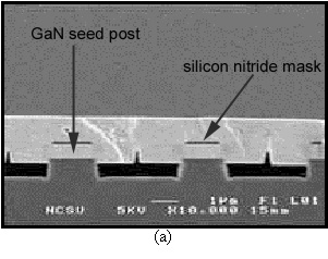
Figure 5a Micrographs taken via cross-sectional SEM of examples of masked pendeo-epitaxial growth with coalescence over and between the seed forms resulting in a single GaN layer.

Figure 5b Micrographs taken via plan-view SEM of examples of masked pendeo-epitaxial growth with coalescence over and between the seed forms resulting in a single GaN layer.
The low-temperature (7K) photoluminescence spectrum of the coalesced PE GaN is shown in Figure 6. The edge emission band (3.454 eV), usually assigned to an exciton bound to a neutral donor (X-D0) is blueshifted −112 meV compared to the GaN seed layer. The common weak yellow band was also observed for the pendeoepitaxial layer. The blueshift is attributed to relaxation of the pendeoepitaxially grown GaN.

Figure 6 Low temperature (7K) photoluminescence spectrum of a coalesced layer of pendeoepitaxial GaN grown on a GaN/AlN/6H-SiC substrate.
3.1.2. Silicon Substrates
Research regarding development of process routes leading to the growth of III-Nitride films on Si has been minimal relative to the number of studies concerned with growth on sapphire and SiC. This has been due in part to the three-dimensional nucleation and growth of GaN islands caused by the combination of significant mismatches in lattice parameters, the higher surface energy of GaN and the chemical reactivity of Si with the reactants in the growth environment. To address the above concerns we have developed a process route similar to those used for growth of GaN on 6H-SiC(0001), but replaced the 6H-SiC substrate with a 3C-SiC(111) transition layer grown on a Si(111) substrate, in the manner discussed in Reference Reference Zorman, Fleischman, Dewa, Mehregany, Jacob, Nishino and Pirouz[28]. The atomic arrangement of the (111) plane of 3C-SiC is equivalent to the (0001) plane of 6H-SiC; this facilitates the sequential deposition of a high temperature 2H-AlN(0001) buffer layer of sufficient quality for the GaN seed layer. As described for the use of the SiC substrates, the 3C-SiC layer must be exposed via etching and the resulting seed forms either capped with a silicon nitride growth mask or left uncapped.
For the initial demonstrations of PE growth of GaN films on silicon, 0.5 and 2 μm thick 3C-SiC layers were deposited on 50 mm diameter, 250 μm thick converted Si(111) substrates. However, the ~0.5 μm 3C-SiC layer cracked on cooling and did not provide an adequate barrier to the reaction with the Si substrate. All subsequent research described below used the ~2.0 μm barrier layer.
Figure 7 shows a cross-sectional SEM micrograph of a PE GaN layer grown laterally and vertically from raised GaN stripes etched in a GaN/AlN/3C-SiC/Si(111) substrate and over the silicon nitride mask atop each stripe. Tilting between adjacent growth fronts over the mask regions are commonly observed in coalesced GaN epilayers grown using the LEO technique. This phenomenon was also determined to be present in the PE GaN films grown on masked seed structures. The splitting of the XRD rocking curves for the (0002) reflection are indicative of the crystallographic tilt and are dependent on the crystal orientation, as shown in Figure 8. The XRD spectrum taken along the [1

Figure 7 Cross-sectional SEM micrograph of a coalesced PE GaN epilayer deposited on a masked GaN/AlN/3C-SiC/Si(111) substrate.

Figure 8. Double crystal XRD analysis of the tilting in the coalesced PE films.
Unlike LEO, coalesced PE GaN epilayers obtained using silicon nitride masks contain two sets of coalesced growth fronts, namely, over the trenches and over the masks. A spatially sensitive method of evaluating the tilt in PE grown GaN is required to determine if it is present at both areas of coalescence. Figure 9(a) shows a typical TEM selected area diffraction pattern taken from a small area of coalescence in a trench region. Figure 9(b) shows the pattern taken near the region of coalescence over the silicon nitride mask. Analysis of these two patterns reveals little evidence of tilt in the laterally grown material over the trenches; however, significant tilt has occurred over the mask regions of the seed structures. The presence of two crystallographic orientations tilted towards each other have also been reported in GaN films grown via lateral epitaxial growth (LEO) Reference Fini, Marchand, Ibbetson, DenBaars, Mishra and Speck[29] Reference Tomiya, Funato, Asatsuma, Hino, Kijima, Asano and Ikeda[30] Reference Fini, Munkholm, Thompson, Stephenson, Eastman, Ramana Murty, Auciello, Zhao, DenBaars and Speck[31] Reference Sakai, Sunakawa, Kimura and Usui[32]. Thus the mask has markedly influenced the crystallographic tilt in the overgrown film. Additional influences of the masks on the quality of the overgrown GaN layer are shown (1) by the voids observed above the masks and similar to those shown in Figure 5 and Figure 7 and (2) the formation of boundaries in the area of coalescence due to the misregistry between the two growth fronts meeting above each mask, as shown in Figure 10. This last figure shows that the growth fronts on both sides of the coalescence boundary are highly defective as a result of the crystallographic misregistry at the boundary. Results similar to these have been reported for GaN films grown via LEO by Lilienthal-Weber, et al. Reference Liliental-Weber, Benamara, Swider, Washburn, Park, Grudowski, Eiting and Dupuis[33]. These problems are also associated with the PE of AlxGa1−xN films with the additional problem of nucleation of AlN on the masks.
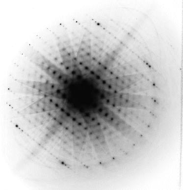
Figure 9a TEM selected area diffraction patterns from (a) a small section of coalesced PE GaN over a trench region and (b) a small area of PE GaN imaged from an area over the silicon nitride mask.

Figure 9b. see caption for Figure 9a

Figure 10. TEM micrograph of a GaN film grown over a silicon nitride mask. The coalescence boundary acted as a nucleation source for horizontally oriented dislocations.
A typical room temperature PL spectrum for a PE GaN film grown on 2 μm wide raised stripes, oriented in the [1

Figure 11. Room temperature photoluminescence of a coalesced layer of PE GaN grown on a GaN/AlN/3C-SiC/Si(111) substrate.

Figure 12. Comparison of low-temperature (14K) PL spectra of PE GaN grown on GaN/AlN/6H-SiC and GaN/AlN/3C-SiC/Si(111) substrates.
3.2 Growth from Unmasked GaN and AlGaN Stripes
3.2.1. Silicon Carbide Substrates
The tilting and consequent void formation, crystallographic misregistry and boundary formation caused by growth over the silicon nitride masks shown by the X-ray and TEM studies discussed above is unacceptable for a semiconductor film on which devices would be fabricated. The advantage of the masks in blocking the vertical propagation of threading dislocations from the initial GaN or AlxGa1−xN stripes in the pendeo-epitaxial areas is outweighed by the formation of the boundaries and the horizontal dislocations due the crystallographic misregistry. As such, the use of masks was discontinued and a variation in the above process route was developed.
Electron beam lithography was applied to reduce the width of the GaN stripes to submicron dimensions, and the masking layer was eliminated. Figure 13(a) shows a GaN film grown from submicron wide, unmasked GaN seed posts on a 6H-SiC substrate. Neither voids nor misregistry above the stripes is visible. The TEM micrograph in Figure 13(b) reveals a significant reduction in the density of vertically oriented threading dislocations in the laterally and vertically grown GaN relative to the stripes. Some dislocations threaded vertically, but with a gradual reduction in density. No dislocations or boundaries were generated within the areas of coalescence over the trench above the void. Selected area diffraction patterns from above the stripes and above the voids showed little evidence of tilt in this film.

Figure 13a. GaN film grown on unmasked, submicron wide stripes of a GaN/AlN/6H-SiC(0001) substrate. No misregistry above the GaN stripes was observed.

Figure 13b. TEM micrograph of the sample shown in (a). A significant reduction in the density of threading dislocations has been obtained in the PE GaN compared to the GaN stripes.
Pendeo-epitaxial films of Al10Ga90N were grown on submicron wide, unmasked GaN stripes on 6H-SiC(0001) substrates, as shown in Figure 14(a) . A large area scan via high resolution Auger electron spectroscopy revealed a variation in the Al content of +/− 0.5% Reference Gehrke, Linthicum and Rajagopal[24]. The elimination of the masking layer was necessary, as AlxGa1−xN nucleates on the silicon nitride mask layer. The TEM micrograph in Figure 14(b) shows no lateral propagation of the vertically oriented threading dislocations in the laterally grown Al10Ga90N regions. Only the threading dislocations within the GaN stripe propagated vertically into the newly deposited GaN. Selected area diffraction in the TEM of the areas of the film coalesced over the Al10Ga90N stripes revealed neither tilting nor a boundary of coalescence, in contrast to those films that coalesced over the silicon nitride masks. The uniform density in the film contrast in Figure 14(b) within the areas of coalesce over the SiC also indicates that no boundary formed in these regions. Dislocations were not observed within the areas of coalescence above the trench of this film. However, threading dislocations, normally stopped by the amorphous silicon nitride mask now extended into the newly deposited films. Preliminary analyses of the GaN seed/GaN PE and the AlN/GaN PE interfaces revealed little evidence of the lateral propagation of these defects.

Figure 14a. Al10Ga90N film grown via pendeo-epitaxy on unmasked GaN seed posts on a 6H-SiC substrate. No misregistry above the GaN seed posts is observable.

Figure 14b. TEM micrograph of the sample in (a). A significant reduction in density of threading dislocations in the pendeo-epitaxial Al10Ga90N compare to the GaN seed post is obvious.
Spatially resolved strain and optical emission plots of stripe and wing regions were produced by micro-Raman and micro-PL measurements at a temperature of 8K. Micro-Raman measurements of an uncoalesced PE GaN Film indicate a shift in the E2 phonon to higher frequency in the wing with respect to the stripe (Figure 15). The shift corresponds to a relaxation in the wing material that is also measured in XRD by a reduction in the lattice parameters, a(−0.07%) and c(+0.03%) in the wing material. The wing material is relaxed with less strain and also emits very sharply in photoluminescence (PL). The donor bound exciton emission peak in the wing material has a FWHM value less than 300 μeV (below the resolution of the equipment) compared to 12 meV for the stripe material as seen in Figure 16. The sharp optical emission from the wing material is comparable to homoepitaxy GaN grown on bulk GaN crystals Reference Kirchner, Schwegler and Eberhard[34]. A downshift in the D0X peak of 5 meV in the post with respect to the wing is due to an increase in tensile strain in the former.

Figure 15. Two-dimensional space plot of Raman line frequency of an uncoalesced PE GaN film (specifically a wing and stripe region). An increase in the line frequency represents a relaxation of strain in the material.

Figure 16. Photoluminescence (PL) spectra taken from the wing and stripe region of an uncoalesced PE GaN film. Note the FWHM value for the wing peak is <300 µeV.
3.2.2. Silicon Substrates
Absence of dislocations in the laterally overgrown material was also obtained for PE GaN films grown laterally and vertically from an unmasked, raised GaN stripe etched into a GaN/AlN/3C-SiC/Si(111) substrate, as shown by a representative sample in Figure 17 (a,b). The TEM image in Figure 17(b) again reveals a significant reduction in density of vertically oriented threading dislocations in the laterally grown GaN region. Some horizontally oriented dislocations that do not propagate to the surface of the film were generated at the GaN/AlN interface of the GaN seed post. Dislocations generated at the GaN/AlN interface in the (0001) planes of the GaN stripes did not propagate vertically to the surface of the film.

Figure 17a. Coalesced GaN films grown on un-masked GaN stripes on a GaN/AlN/3C-SiC/Si(111) substrate. No misregistry above the GaN seed post was observed.

Figure 17b. TEM micrograph of the sample in (a). A significant reduction in density of threading dislocations occurred in the pendeo-epitaxial GaN compared to the GaN stripes.
4. Summary
Pendeo-epitaxy has been developed as an alternative and more simple approach of growing uniformly thin films with low densities of threading dislocations over the entire surface of a substrate. In particular, the growth of both discrete structures and coalesced GaN and AlxGa1−xN films and multilayer heterostructures using pendeo-epitaxy on etched GaN seed layers previously grown on AlN(0001)/6H-SiC(0001) and AlN(0001)/SiC(111)/Si(111) substrates has been demonstrated. Tilting in the coalesced GaN epilayers of 0.2° was confined to areas of mask overgrowth; very little tilting was observed in the material suspended above the trenches or grown over unmasked stripes. The strong, low-temperature PL band-edge peak at 3.45 eV with a FWHM of <300 µeV was measured in the overgrowth GaN material. The band-edge in the material on Si(111) was shifted by 10 meV to a lower energy, indicative of a greater tensile stress.
ACKNOWLEDGMENTS
The authors acknowledge Cree Research, Inc. for the SiC wafers. This work was supported by the Office of Naval Research under contracts N00014-98-1-0384 (Colin Wood, monitor) and N00014-98-1-0654 (John Zolper, monitor) as well as The Kenan Institute for Engineering, Technology and Science at NCSU. R.F. Davis was supported in part by the Kobe Steel, Ltd. Professorship. The authors also acknowledge the Georgia Technology Research Institute for use of their clean room facilities.


