


I. INTRODUCTION
Fast X-ray fluorescence (XRF) element mapping coupled with a submicrometer-sized X-ray beam (utilizing JTEC KB mirrors at a flux of some 1010 ph s−1 in an energy range of 5–21 keV) characterizes the basic experiment in the microprobe hutch of the Hard X-Ray Micro/Nano-Probe beamline P06 at PETRA III (DESY) (Boesenberg et al., Reference Boesenberg, Ryan, Kirkham, Siddons, Alfeld, Garrevoet, Núñez, Claussen, Kracht and Falkenberg2016). Modes of operation are two-dimensional lateral scanning (Carmona et al., Reference Carmona, Zogzas, Roudeau, Porcaro, Garrevoet, Spiers, Salomé, Cloetens, Mukhopadhy and Ortega2019), (XRF-) tomography of virtual slices (Mishra et al., Reference Mishra, Alfeld, Sobotka, Andresen, Falkenberg and Küpper2016), and, on smaller particles, real three-dimensional scanning XRF tomography (Kalirai et al., Reference Kalirai, Boesenberg, Falkenberg, Meirer and Weckhuysen2015). Spectro-microscopic XANES imaging by creating energy stacks of 2D element maps (Monico et al., Reference Monico, Janssens, Hendriks, Vanmeert, Van der Snickt, Cotte, Falkenberg, Brunetti and Miliani2015) has recently been advanced to XANES tomography of virtual slices (Mijovilovich et al., Reference Mijovilovich, Mishra, Brückner, Spiers, Andresen, Garrevoet, Falkenberg and Küpper2019). Scanning XRF can be complemented by (powder) X-ray diffraction (Vanmeert et al., Reference Vanmeert, Van der Snickt and Janssens2015; Wittig et al., Reference Wittig, Palle, Østergaard, Frølich, Birkbak, Spiers, Garrevoet and Birkedal2019) for simultaneous imaging of structure and element composition since the advent of fast hybrid pixel detectors with millisecond dwell time like the Pilatus 300k, Lambda and Eiger X 4M at P06. The small pixel size of the Eiger detector together with a large propagation distance made fast ptychographic measurements possible at the Microprobe. The large focal distance of the Kirkpatrick-Baez (KB) system allows the implementation of various sample environments like cryostreams, cryogenic sample chambers, chemical reactors, diamond anvil cells, and other user supplied equipment.
The recent innovation of phase plates for the aberration correction of X-ray optics (Seiboth et al., Reference Seiboth, Schropp, Scholz, Wittwer, Rödel, Wünsche, Ullsperger, Nolte, Rahomaki, Parfeniukas, Giakoumidis, Vogt, Wagner, Rau, Boesenberg, Garrevoet, Falkenberg, Galtier, Lee, Nagler and Schroer2017) made the application of compound refractive lenses (CRsL) attractive as the complementation of the KB system for focusing down to 100 nm beamsize at intermediate energies (8–20 keV) (Schropp et al., Reference Schropp, Bruckner, Bulda, Falkenberg, Garrevoet, Seiboth, Wittwer, Koch, David and Schroer2018). The 100-nm beam with large focal distance has enabled multimodal measurements on solar cells including X-ray beam-induced current (Ossig et al., Reference Ossig, Nietzold, West, Bertoni, Falkenberg, Schroer and Stuckelberger2019) and X-ray excited optical luminescence in addition to XRF and ptychography. However, the same setup and technology allows, with more lenses and a modified phase plate, also submicrometer focusing at 35 keV. The high-energy microprobe setup was initiated for scanning (powder) X-ray diffraction studies of highly absorbing (paint-) samples and K-edge XRF measurements of heavier elements from silver to iodine in bio-medical applications, but meanwhile attracted interest also for applications in materials sciences and catalysis research.
In general, submicrometer beam setups at high energies above 30 keV are rare due to lower flux and coherence of the X-ray sources and lower efficiency of X-ray optics and X-ray detectors. Several high-energy beamlines at high-energy storage rings like 16-ID-B at APS, P02.2 at PETRA III, BL37XU at Spring-8, and ID16A at ESRF are based on dedicated KB mirror systems and obtain focus sizes in the low micrometer range, and even below 20 nm in case of ID16A (da Silva et al., Reference da Silva, Pacureanu, Yang, Bohic, Morawe, Barrett and Cloetens2017). Other beamlines use CRL optics, for example ID15b and ID31 at ESRF or P02.2, P07, and P21 at PETRA III (DESY). CRLs are known for their ease of installation, alignment, and beam stability, but beam sizes are several micrometer and above at these high-energy beamlines, partly due to spherical aberrations of the CRL.
In this paper, we report on the performance of a provisional setup for microprobe experiments at 35 keV. Phase plate-corrected CRL optics at 35 keV were characterized by ptychography and XRF edge scans on a siemens star pattern. Also, a Vortex silicon drift detector (SDD) with 2 mm sensor thickness for increased sensitivity at high energies was successfully tested. The performance of the new high-energy setup for microscopic X-ray powder diffraction (XRD)–XRF scanning X-ray microscopy measurements is demonstrated on a cross-section of a painting fragment.
II. EXPERIMENTAL
A. The test setup
The target energy of 35 keV lies well within the energy range of the beamline optics of P06 including undulator and a cryo-cooled Si111 monochromator, but is beyond the cutoff energy of the KB system. The setup at the microprobe experiment allows the motorized translation of the KB optics box out of the beam and an easy installation of a stack of stages for x, y, z translations and ϕ and θ rotations for the alignment of the CRL. The focal distance of 149 CRL at 35 keV was 660 mm measured from the exit of the N2-rinsed CRL box (see Figure 1). The corrective phase plate, which is located downstream outside of the CRL box, is positioned by a smaract xyz piezopositioner. The standard Vortex EM (Hitachi High-Tech) SDD with 0.5 mm sensor thickness is exchanged with a prototype Vortex SDD with 2 mm sensor thickness. Both detectors use an Xspress 3 X-ray fluorescence detector readout system (Quantum Detectors Ltd). Instead of the standard Si-based Eiger 4M hybrid pixel detector (Dectris), a GaAs Lambda 2M detector (XSPECTRUM) was used for XRD (at a 0.1 m sample–detector distance) and ptychography (at a 8.5 m sample–detector distance).
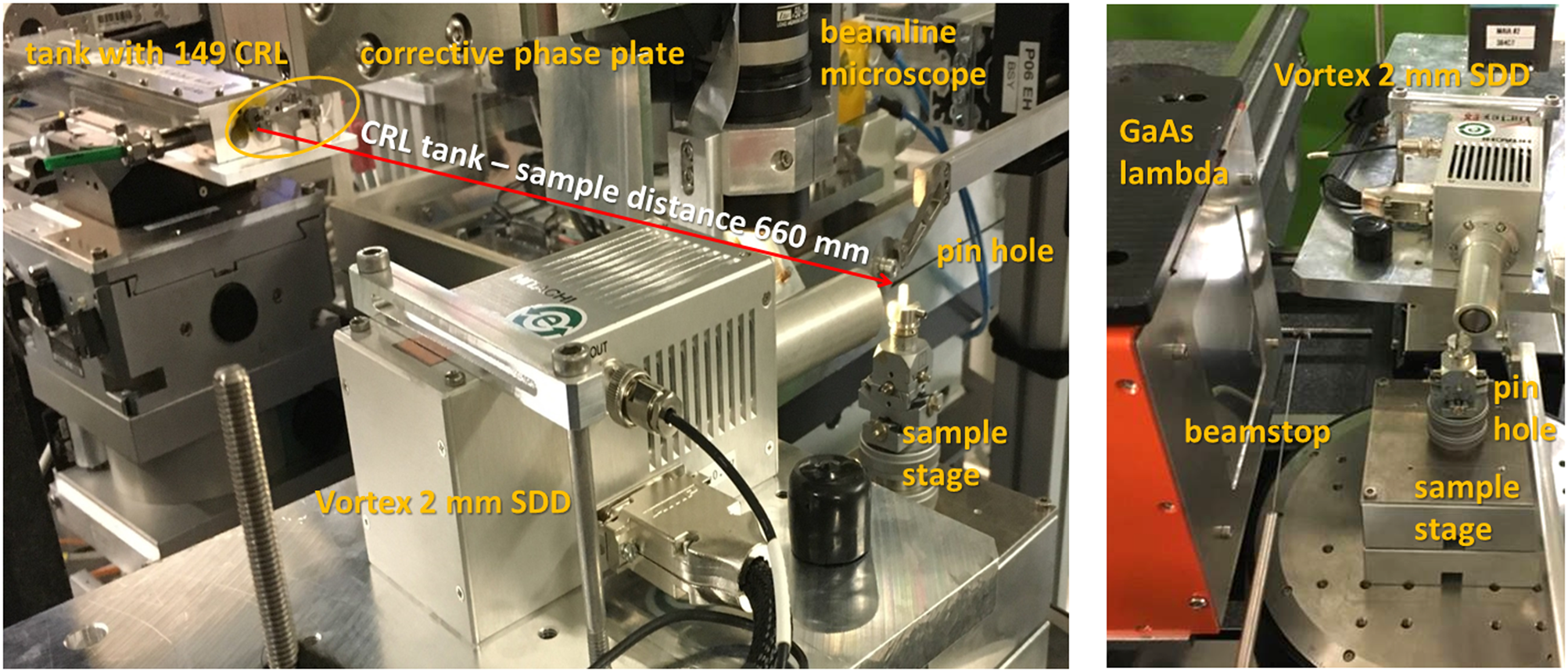
Figure 1. P06 Microprobe test setup for 35 keV operation. (left) The 35 keV X-ray beam is focused by 149 Be CRLs to the sample position. The wavefront is corrected by a phase plate-positioned downstream, close to the CRL box. (right) For micro-XRD measurements, the GaAs lambda detector is positioned close to the sample.
B. X-ray optics
A 149 parabolic 2D Beryllium CRL [radius of curvature R 0 50 μm, material IF1 (RXOPTICS GmbH, Germany)] terminated on both sides with pinholes of 0.4 mm inner diameter was stacked on top of two precisely machined parallel cylinders inside a steel box with gas inlets and kapton windows (RXOPTICS). This simple and compact solution assures precise on-axis alignment of CRL for the complete stack at once. The application of a transfocator was resigned due to space limitations and simplicity. Energy changes over a limited range of several keV were enabled by shifting the CRL box position along the beam direction. The CRLs were aligned for maximum symmetry of the pinhole shape silhouette in the far field image detected with a PCO 4000 CDD camera and an Optique Peter scintillator-based optics. Also, the correction-phase plate was aligned for maximum symmetry of the far field image. Note that the beam shape is sensitive to 1 μm misplacement of the correction-phase plate alignment.
C. X-ray detectors
Standard Si-based X-ray detectors have sensor thicknesses of 0.5 mm, which result in reduced sensitivity at energies above 10 keV. At 35 keV only, about 11% of the X-ray photons are absorbed within the sensor (see Table I). The stopping power can be increased by selecting a sensor material of higher atomic mass (like GaAs of the lambda detector for diffraction) or by increasing the Si sensor thickness. Hitachi High-Tech has developed a new Vortex Si drift detector with 2 mm sensor thickness, which we were allowed to use for our test measurements.
TABLE I. Absorption within the Si detector material of 0.5 and 2 mm thickness (calc. by XOP 2.4).

III. RESULTS
A. X-ray optics
A siemens star test pattern (XRESO-50HC, NTT-AT) was scanned through the X-ray focus for the characterization of the X-ray beam by ptychography in a high coherence condition [front-end slit size 0.5 × 0.04 mm2 (vertical × horizontal)] and by XRF edge scans at various slit sizes. The ptychography results [see Figures 2(a)–2(d)] show that the (coherent) size of the central cone is about 110 nm [as only the dominant mode is used for reconstruction (da Silva et al., Reference da Silva, Pacureanu, Yang, Bohic, Morawe, Barrett and Cloetens2017)]. The aberrations of the focused beam can be efficiently corrected by the phase plate. The dependence of the focus size and flux at the sample on the front-end slit size is listed in Table II. Note that the flux can be further increased on the expense of the focus size by the application of upstream prefocusing CRL.

Figure 2. Characterization of the focused X-ray beam at 35 keV by ptychography and XRF edge scans on a siemens star test pattern. (a) and (b) show the caustic of the reconstructed beam with and without phase plate for aberration correction; (c) and (d) show the corresponding beam cross-section at the focus position. The size of the (incoherent) beam depends on the opening of the horizontal front-end slits. Edge scans across the edges of a siemens star pattern and their derivative are shown in (e) and (f).
TABLE II. Focal size and flux depend strongly on the opening of the front-end slits.

B. X-ray detectors
The new Vortex with 2 mm sensor thickness was compared with a standard Vortex EM detector with 0.5 mm sensor thickness. A multi-element standard reference sample AXO RF17 15C10 and a clean Si block (“blank”) were measured with both detectors under identical conditions at 35 keV excitation energy. The Vortex 2 mm detector showed the expected increase in sensitivity at high energies [see Figure 3(a)]. Very important for ultra-trace element analysis is the cleanliness of the blank spectrum. The spectrum recorded on the blank did not show XRF lines for the Vortex 2 mm, but for the Vortex 0.5 mm. Those lines (“contamination”) originate from the detector material which is insufficiently shielded against the high-energy scatter radiation. The slightly degraded energy resolution and background can be attributed to nonoptimized settings of the Xspress 3 detector readout (Quantum Detectors Ltd).

Figure 3. Spectra taken with Vortex EM 0.5 mm and Vortex 2 mm under comparable conditions. (a) Multielement standard AXO RF17 15C10 and (b) clean thick silicon (“blank”).
C. Application: combined XRD–XRF scan on a painting fragment
The applicability of the new test setup for microscopic XRD–XRF scanning X-ray microscopy measurements at 35 keV was tested on a cross-section of a painting fragment that was measured at 21 keV at the P06 Microprobe experiment before. A comparison showed that the angular resolution in XRD was comparable, but a few components were only detectable at 21 keV due to higher flux. Cd could be detected in XRF only at high energies (Figure 4). High energies are expected to be superior in XRD for thicker samples of high density material, e.g. paintings including white lead layers or the investigation of metals.

Figure 4. XRD–XRF scan on a painting cross-section: scan area 150 × 30 μm2, 1 μm steps, and 6 s dwelltime.
IV. CONCLUSION
A temporary setup for scanning X-ray microscopy at 35 keV was tested at the beamline P06 Microprobe. Using CRL with phase correction, a nanofocus with sizes down to 250 nm (110 nm coherent) could be achieved. A prototype Hitachi High-Tech Vortex SDD with 2 mm sensor thickness was successfully tested for XRF mapping with increased sensitivity at high energies. The high-energy setup will be available for users after implementation of a dedicated CRL stage with short conversion time to KB mirror operation, probably in spring 2021. Potential applications include nano-XRD (tomography) on highly absorbing samples like metals or thick painting fragments; also heavily absorbing sample environments like diamond anvil cells or chemical reactors. The high excitation energy makes it also possible to access K-edges of Cd to I for nano-XRF (tomography). Eventually, the energy can be increased beyond 35 keV in order to include also K-edges of light rare earth elements.
ACKNOWLEDGEMENTS
Beamtime at beamline P06 at PETRA III was granted within the in-house research program of DESY, a member of the Helmholtz-Association. We thank Hitachi High-Tech for the loan of the prototype detector and Koen Janssens (University of Antwerp) for providing the paint sample fragment. All figures and pictures were provided by the author(s) under a CC BY 4.0 licence (https://creativecommons.org/licenses/by/4.0/).


 Open access