Hostname: page-component-8448b6f56d-dnltx Total loading time: 0 Render date: 2024-04-18T13:55:55.837Z Has data issue: false hasContentIssue false

Mechanism-based design of precursors for focused electron beam-induced deposition

Published online by Cambridge University Press:  26 April 2018

Will G. Carden
Affiliation:
Department of Chemistry, University of Florida, Gainesville, Florida 32611-7200, USA
Hang Lu
Affiliation:
Department of Chemistry, University of Florida, Gainesville, Florida 32611-7200, USA
Julie A. Spencer
Affiliation:
Department of Chemistry, Johns Hopkins University, Baltimore, Maryland 21218-2685, USA Department of Chemistry, United States Naval Academy, Annapolis, Maryland 21402, USA
D. Howard Fairbrother
Affiliation:
Department of Chemistry, Johns Hopkins University, Baltimore, Maryland 21218-2685, USA
Lisa McElwee-White*
Affiliation:
Department of Chemistry, University of Florida, Gainesville, Florida 32611-7200, USA
*
Address all correspondence to Lisa McElwee-White at lmwhite@chem.ufl.edu
Get access

Abstract

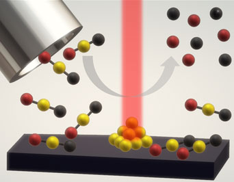
Focused electron beam-induced deposition (FEBID) is capable of producing metal-containing nanostructures with lateral resolution on the sub-nanometer scale. Practical application of this nanofabrication technique has been hindered by ligand-derived contamination from precursors developed for thermal deposition methods. Mechanistic insight into FEBID through surface science studies and gas-phase electron–molecule interactions has begun to enable the design of custom FEBID precursors. These studies have shown that precursors designed to decompose under electron irradiation can produce high-purity FEBID deposits. Herein, we highlight the progress in FEBID precursor development with several examples that incorporate this mechanism-based design approach.

Type
Prospective Articles
Copyright
Copyright © Materials Research Society 2018 

Access options

Get access to the full version of this content by using one of the access options below. (Log in options will check for institutional or personal access. Content may require purchase if you do not have access.)

References

1.van Dorp, W., Hagen, C., Crozier, P., and Kruit, P.: Growth behavior near the ultimate resolution of nanometer-scale focused electron beam-induced deposition. Nanotechnology 19, 225305 (2008).CrossRefGoogle ScholarPubMed
2.Randolph, S.J., Fowlkes, J.D., and Rack, P.D.: Focused, nanoscale electron-beam-induced deposition and etching. Crit. Rev. Solid State Mater. Sci. 31, 55 (2006).Google Scholar
3.van Dorp, W.F. and Hagen, C.W.: A critical literature review of focused electron beam induced deposition. J. Appl. Phys. 104, 081301 (2008).CrossRefGoogle Scholar
4.Utke, I., Hoffman, P., and Melngailis, J.: Gas-assisted focused electron beam and ion beam processing and fabrication. J. Vac. Sci. Technol. B 26, 1197 (2008).Google Scholar
5.Huth, M., Porrati, F., Schwalb, C., Winhold, M., Sachser, R., Dukic, M., Adams, J., and Fantner, G.: Focused electron beam induced deposition: a perspective. Beilstein J. Nanotechnol. 3, 597 (2012).CrossRefGoogle ScholarPubMed
6.Acar, H.: Fabrication of plasmonic nanostructures with electron beam induced deposition (University of Twente, Zutphen, 2013).Google Scholar
7.Gavagnin, M., Wanzenboeck, H.D., Belic, D., and Bertagnolli, E.: Synthesis of individually tuned nanomagnets for nanomagnet logic by direct write focused electron beam induced deposition. ACS Nano 7, 777 (2013).CrossRefGoogle ScholarPubMed
8.Brown, J., Kocher, P., Ramanujan, C.S., Sharp, D.N., Torimitsu, K., and Ryan, J.F.: Electrically conducting, ultra-sharp, high aspect-ratio probes for AFM fabricated by electron-beam-induced deposition of platinum. Ultramicroscopy 133, 62 (2013).Google Scholar
9.Murakami, K. and Takai, M.: Characteristics of nano electron source fabricated using beam assisted process. J. Vac. Sci. Technol. B 22, 1266 (2004).CrossRefGoogle Scholar
10.Murakami, K. and Takai, M.: Nano electron source fabricated by beam-induced deposition and its unique feature. Microelectron. Eng. 132, 74 (2015).Google Scholar
11.Perentes, A. and Hoffmann, P.: Focused electron beam induced deposition of Si-based materials from SiOxCy to stoichiometric SiO2: chemical compositions, chemical-etch rates, and deep ultraviolet optical transmissions. Chem. Vap. Deposition 13, 176 (2007).Google Scholar
12.Edinger, K., Becht, H., Bihr, J., Boegli, V., Budach, M., Hofmann, T., Koops, H.W.P., Kuschnerus, P., Oster, J., Spies, P., and Weyrauch, B.: Electron-beam-based photomask repair. J. Vac. Sci. Technol. B 22, 2902 (2004).Google Scholar
13.Liang, T., Frendberg, E., Lieberman, B., and Stivers, A.: Advanced photolithographic mask repair using electron beams. J. Vac. Sci. Technol. B 23, 3101 (2005).Google Scholar
14.Heerkens, C.T.H., Kamerbeek, M.J., van Dorp, W.F., Hagen, C.W., and Hoekstra, J.: Electron beam induced deposited etch masks. Microelectron. Eng. 86, 961 (2009).Google Scholar
15.Hubner, B., Koops, H.W.P., Pagnia, H., Sotnik, N., Urban, J., and Weber, M.: Tips for scanning tunneling microscopy produced by electron-beam-induced deposition. Ultramicroscopy 42–44, 1519 (1992).Google Scholar
16.Chen, I.-C., Chen, L.-H., Orme, C., Quist, A., Lal, R., and Jin, S.: Fabrication of high-aspect-ratio carbon nanocone probes by electron beam induced deposition patterning. Nanotechnology 17, 4322 (2006).Google Scholar
17.Graells, S., Alcubilla, R., Badenes, G., and Quidant, R.: Growth of plasmonic gold nanostructures by electron beam induced deposition. Appl. Phys. Lett. 91, 121112 (2007).Google Scholar
18.Weber-Bargioni, A., Schwartzberg, A., Schmidt, M., Harteneck, B., Ogletree, D.F., Schuck, P.J., and Cabrini, S.: Functional plasmonic antenna scanning probes fabricated by induced-deposition mask lithography. Nanotechnology 21, 065306 (2010).Google Scholar
19.Koops, H.W.P., Hoinkis, O.E., Honsberg, M.E.W., Schmidt, R., Blum, R., Bottger, G., Kuligk, A., Liguda, C., and Eich, M.: Two-dimensional photonic crystals produced by additive nanolithography with electron beam-induced deposition act as filters in the infrared. Microelectron. Eng. 57–8, 995 (2001).Google Scholar
20.Basu, J., Carter, D.B., Divakar, R., Shenoy, V.B., and Ravishankar, N.: Modified electron-beam-induced deposition of metal nanostructure arrays using a parallel electron beam. Appl. Phys. Lett. 93, 133104/1 (2008).Google Scholar
21.Fowlkes, J.D., Winkler, R., Lewis, B.B., Stanford, M.G., Plank, H., and Rack, P.D.: Simulation-guided 3D nanomanufacturing via focused electron beam induced deposition. ACS Nano 10, 6163 (2016).CrossRefGoogle ScholarPubMed
22.Winkler, R., Schmidt, F.-P., Haselmann, U., Fowlkes, J.D., Lewis, B.B., Kothleitner, G., Rack, P.D., and Plank, H.: Direct-write 3D nanoprinting of plasmonic structures. ACS Appl. Mater. Interfaces 9, 8233 (2017).Google Scholar
23.McElwee-White, L., Koller, J., Kim, D., and Anderson, T.J.: Mechanism-based design of precursors for MOCVD. ECS Trans. 25, 161 (2009).CrossRefGoogle Scholar
24.McElwee-White, L.: Design of precursors for the CVD of inorganic thin films. Dalton Trans., 5327 (2006).Google Scholar
25.Wnuk, J.D., Gorham, J.M., Rosenberg, S.G., van Dorp, W.F., Madey, T.E., Hagen, C.W., and Fairbrother, D.H.: Electron induced surface reactions of the organometallic precursor trimethyl(methylcyclopentadienyl)platinum(IV). J. Phys. Chem. C 113, 2487 (2009).Google Scholar
26.Wnuk, J.D., Rosenberg, S.G., Gorham, J.M., van Dorp, W.F., Hagen, C.W., and Fairbrother, D.H.: Electron beam deposition for nanofabrication: insights from surface science. Surf. Sci. 605, 257 (2011).Google Scholar
27.Silvis-Cividjian, N., Hagen, C.W., and Kruit, P.: Spatial resolution limits in electron-beam-induced deposition. J. Appl. Phys. 98, 084905 (2005).Google Scholar
28.Botman, A., Winter, D.A.M.D., and Mulders, J.J.L.: Electron-beam-induced deposition of platinum at low landing energies. J. Vac. Sci. Technol. B 26, 2460 (2008).Google Scholar
29.Thorman, R.M., Kumar, T.P.R., Fairbrother, D.H., and Ingolfsson, O.: The role of low-energy electrons in focused electron beam induced deposition: four case studies of representative precursors. Beilstein J. Nanotechnol. 6, 1904 (2015).Google Scholar
30.Botman, A., Hesselberth, M., and Mulders, J.J.L.: Investigation of morphological changes in platinum-containing nanostructures created by electron-beam-induced deposition. J. Vac. Sci. Technol. B 26, 2464 (2008).Google Scholar
31.Henderson, M.A., Ramsier, R.D., and Yates, J.T.: Low-energy electron induced decomposition of Fe(CO)5 adsorbed on Ag(111). Surf. Sci. 259, 173 (1991).Google Scholar
32.Córdoba, R., Sesé, J., De Teresa, J.M., and Ibarra, M.R.: High-purity cobalt nanostructures grown by focused-electron-beam-induced deposition at low current. Microelectron. Eng. 87, 1550 (2010).Google Scholar
33.Weber, M., Koops, H.W.P., Rudolph, M., Kretz, J., and Schmidt, G.: New compound quantum dot materials produced by electron-beam induced deposition. J. Vac. Sci. Technol. B 13, 1364 (1995).Google Scholar
34.Porrati, F., Sachser, R., and Huth, M.: The transient electrical conductivity of W-based electron-beam-induced deposits during growth, irradiation and exposure to air. Nanotechnology 20, 195301 (2009).Google Scholar
35.Rack, P.D., Randolph, S., Deng, Y., Fowlkes, J., Choi, Y., and Joy, D.C.: Nanoscale electron-beam-stimulated processing. Appl. Phys. Lett. 82, 2326 (2003).Google Scholar
36.Mulders, J.J.L., Belova, L.M., and Riazanova, A.: Electron beam induced deposition at elevated temperatures: compositional changes and purity improvement. Nanotechnology 22, 055302 (2011).Google Scholar
37.Koops, H.W.P., Weiel, R., Kern, D.P., and Baum, T.H.: High-resolution electron-beam induced deposition. J. Vac. Sci. Technol. B 6, 477 (1988).Google Scholar
38.Rosenberg, S.G., Barclay, M., and Fairbrother, D.H.: Electron induced reactions of surface adsorbed tungsten hexacarbonyl (W(CO)6). Phys. Chem. Chem. Phys. 15, 4002 (2013).Google Scholar
39.Rosenberg, S.G., Barclay, M., and Fairbrother, D.H.: Electron beam induced reactions of adsorbed cobalt tricarbonyl nitrosyl (Co(CO)3NO) molecules. J. Phys. Chem. C 117, 16053 (2013).Google Scholar
40.Rosenberg, S.G., Barclay, M., and Fairbrother, D.H.: Electron induced surface reactions of organometallic metal(hfac)2 precursors and deposit purification. ACS Appl. Mater. Interfaces 6, 8590 (2014).Google Scholar
41.Wnuk, J.D., Gorham, J.M., Rosenberg, S.G., van Dorp, W.F., Madey, T.E., Hagen, C.W., and Fairbrother, D.H.: Electron beam irradiation of dimethyl-(acetylacetonate) gold(III) adsorbed onto solid substrates. J. Appl. Phys. 107, 054301/1 (2010).Google Scholar
42.Barry, J.D., Ervin, M.H., Molstad, J., Wickenden, A., Brintinger, T., Hoffman, P., and Meingailis, J.: Electron beam induced deposition of low resistivity platinum from Pt(PF3)4. J. Vac. Sci. Technol. B 24, 3165 (2006).CrossRefGoogle Scholar
43.Wang, S., Sun, Y.M., Wang, Q., and White, J.M.: Electron-beam induced initial growth of platinum films using Pt(PF3)4. J. Vac. Sci. Technol. B 22, 1803 (2004).Google Scholar
44.Landheer, K., Rosenberg, S., Bernau, L., Swiderek, P., Utke, I., Hagen, C., and Fairbrother, D.H.: Low-energy electron-induced decomposition and reactions of adsorbed tetrakis(trifluorophosphine)platinum [Pt(PF3)4]. J. Phys. Chem. C 115, 17452 (2011).CrossRefGoogle Scholar
45.Spencer, J.A., Rosenberg, S., Barclay, M., Wu, Y.-C., McElwee-White, L., and Fairbrother, D.H.: Understanding the electron stimulated surface reactions of organometallic complexes to enable design of precursors for electron beam induced deposition. Appl. Phys. A Mater. Sci. Process. 117, 1631 (2014).Google Scholar
46.Jeon, N.L., Lin, W., Erhardt, M.K., Girolami, G.S., and Nuzzo, R.G.: Selective chemical vapor deposition of platinum and palladium directed by monolayers patterned using microcontact printing. Langmuir 13, 3833 (1997).Google Scholar
47.Luisier, A., Utke, I., Bret, T., Cicoira, F., Hauert, R., Rhee, S.W., Doppelt, P., and Hoffmann, P.: Comparative study of Cu-precursors for 3D focused electron beam induced deposition. J. Electrochem. Soc. 151, C590 (2004).Google Scholar
48.Miyazoe, H., Utke, I., Kikuchi, H., Kiriu, S., Friedli, V., Michler, J., and Terashima, K.: Improving the metallic content of focused electron beam-induced deposits by a scanning electron microscope integrated hydrogen-argon microplasma generator. J. Vac. Sci. Technol. B 28, 744 (2010).Google Scholar
49.Laibinis, P.E., Graham, R.L., Biebuyck, H.A., and Whitesides, G.M.: X-Ray damage to CF3CO2-terminated organic monolayers on Si/Au––principal effect of electrons. Science 254, 981 (1991).Google Scholar
50.Perry, C.C., Wagner, A.J., and Fairbrother, D.H.: Electron stimulated C-F bond breaking kinetics in fluorine-containing organic thin films. Chem. Phys. 280, 111 (2002).CrossRefGoogle Scholar
51.Xue, Z., Strouse, M.J., Shuh, D.K., Knobler, C.B., Kaesz, H.D., Hicks, R.F., and Williams, R.S.: Characterization of (methylcyclopentadienyl)trimethylplatinum and low-temperature organometallic chemical vapor deposition of platinum metal. J. Am. Chem. Soc. 111, 8779 (1989).Google Scholar
52.Spencer, J.A., Brannaka, J.A., Barclay, M., McElwee-White, L., and Fairbrother, D.H.: Electron induced surface reactions of η 3-allyl ruthenium tricarbonyl bromide [(η 3-C3H5)Ru(CO)3Br]: contrasting the behavior of different ligands. J. Phys. Chem. C 119, 1534915359 (2015).Google Scholar
53.Thorman, R.M., Brannaka, J.A., McElwee-White, L., and Ingolfsson, O.: Low energy electron-induced decomposition of (η3-C3H5)Ru(CO)3Br, a potential focused electron beam induced deposition precursor with a heteroleptic ligand set. Phys. Chem. Chem. Phys. 19, 13264 (2017).Google Scholar
54.Cotton, F.A., Wilkinson, G., Murillo, C., and Bochmann, M.: Advanced Inorganic Chemistry, 6th ed. (Wiley, New York, 1999).Google Scholar
55.Spencer, J.A., Wu, Y.C., McElwee-White, L., and Fairbrother, D.H.: Electron induced surface reactions of cis-Pt(CO)2Cl2: a route to focused electron beam induced deposition of pure Pt nanostructures. J. Am. Chem. Soc. 138, 9172 (2016).Google Scholar
56.Spencer, J.A., Barclay, M., Gallagher, M.J., Winkler, R., Unlu, I., Wu, Y.-C., Plank, H., McElwee-White, L., and Fairbrother, D.H.: Comparing postdeposition reactions of electrons and radicals with Pt nanostructures created by focused electron beam induced deposition. Beilstein J. Nanotechnol. 8, 2410 (2017).Google Scholar
57.Warneke, J., Rohdenburg, M., Zhang, Y., Orszagh, J., Vaz, A., Utke, I., De Hosson, J.T.M., van Dorp, W.F., and Swiderek, P.: Role of NH3 in the electron-induced reactions of adsorbed and solid cisplatin. J. Phys. Chem. C 120, 4112 (2016).Google Scholar
58.Kopyra, J., Koenig-Lehmann, C., Bald, I., and Illenberger, E.: A single slow electron triggers the loss of both chlorine atoms from the anticancer drug cisplatin: implications for chemoradiation therapy. Angew. Chem. Int. Ed. 48, 7904 (2009).Google Scholar
59.Pham, S.N., Kuether, J.E., Gallagher, M.J., Hernandez, R.T., Williams, D.N., Zhi, B., Mensch, A.C., Hamers, R.J., Rosenzweig, Z., Fairbrother, H., Krause, M.O.P., Feng, Z.V., and Haynes, C.L.: Carbon dots: a modular activity to teach fluorescence and nanotechnology at multiple levels. J. Chem. Ed. 94, 1143 (2017).Google Scholar
60.Naik, G.V., Shalaev, V.M., and Boltasseva, A.: Alternative Plasmonic Materials: Beyond Gold and Silver. Adv. Mater. 25, 3264 (2013).Google Scholar
61.Baum, T.H.: Laser chemical vapor deposition of gold: the effect of organometallic structure. J. Electrochem. Soc. 134, 2616 (1987).Google Scholar
62.Koops, H.W.P., Kretz, J., Rudolph, M., Weber, M., Dahm, G., and Lee, K.L.: Characterization and application of materials grown by electron-beam-induced deposition. Jpn. J. Appl. Phys. 33, 7099 (1994).Google Scholar
63.Utke, I., Jenke, M.G., Roling, C., Thiesen, P.H., Iakovlev, V., Sirbu, A., Mereuta, A., Caliman, A., and Kapon, E.: Polarisation stabilisation of vertical cavity surface emitting lasers by minimally invasive focused electron beam triggered chemistry. Nanoscale. 3, 2718 (2011).Google Scholar
64.Jenke, M.G., Lerose, D., Niederberger, C., Michler, J., Christiansen, S., and Utke, I.: Toward local growth of individual nanowires on three-dimensional microstructures by using a minimally invasive catalyst templating method. Nano Lett. 11, 4213 (2011).Google Scholar
65.Folch, A., Servat, J., Esteve, J., Tejada, J., and Seco, M.: High-vacuum versus “environmental” electron beam deposition. J. Vac. Sci. Technol. B 14, 2609 (1996).Google Scholar
66.Brintlinger, T., Fuhrer, M.S., Melngailis, J., Utke, I., Bret, T., Perentes, A., Hoffmann, P., Abourida, M., and Doppelt, P.: Electrodes for carbon nanotube devices by focused electron beam induced deposition of gold. J. Vac. Sci. Technol. B 23, 3174 (2005).Google Scholar
67.Hoffmann, P., Utke, I., Cicoira, F., Dwir, B., Leifer, K., Kapon, E., and Doppelt, P.: Focused electron beam induced deposition of gold and rhodium. Mater. Res. Soc. Symp. Proc. 624, 171 (2001).Google Scholar
68.Utke, I., Hoffmann, P., Dwir, B., Leifer, K., Kapon, E., and Doppelt, P.: Focused electron beam induced deposition of gold. J. Vac. Sci. Technol. B 18, 3168 (2000).Google Scholar
69.Utke, I., Dwir, B., Leifer, K., Cicoira, F., Doppelt, P., Hoffmann, P., and Kapon, E.: Electron beam induced deposition of metallic tips and wires for microelectronics applications. Microelectron. Eng. 53, 261 (2000).Google Scholar
70.Fuß, W. and Rühe, M.: Chlor(trifluorphosphan)gold(I), eine einfache flüchtige Goldverbindung. Z. Naturforsch. B 47, 591 (1992).Google Scholar
71.Mulders, J.J.L., Veerhoek, J.M., Bosch, E.G.T., and Trompenaars, P.H.F.: Fabrication of pure gold nanostructures by electron beam induced deposition with Au(CO)Cl precursor: deposition characteristics and primary beam scattering effects. J. Phys. D Appl. Phys. 45, 475301 (2012).Google Scholar
72.Jones, P.G.: The crystal structure of carbonyl gold(I) chloride, (OC)AuCl. Z. Naturforsch. B 37, 823 (1982).Google Scholar
73.Belli Dell'Amico, D. and Calderazzo, F.: Convenient methods for the preparation of anhydrous gold(III) chloride and chlorocarbonylgold(I). Gazz. Chim. Ital. 103, 1099 (1973).Google Scholar
74.Tran, P.D. and Doppelt, P.: Gold CVD using trifluorophosphine gold(I) chloride precursor and its toluene solutions. J. Electrochem. Soc. 154, D520 (2007).Google Scholar
75.Kharasch, M.S. and Isbell, H.S.: Chemistry of organic gold compounds. I. Aurous chloride carbonyl and a method of linking carbon to carbon. J. Am. Chem. Soc. 52, 2919 (1930).Google Scholar
76.van Dorp, W., Wu, X., Mulders, J., Harder, S., Rudolf, P., and De Hosson, J.: Gold complexes for focused-electron-beam-induced deposition. Langmuir 30, 12097 (2014).Google Scholar
77.Carden, W.G., Pedziwiatr, J., Abboud, K.A., and McElwee-White, L.: Halide effects on the sublimation temperature of X–Au–L complexes: implications for their use as precursors in vapor phase deposition methods. ACS Appl. Mater. Interfaces 9, 40998 (2017).Google Scholar
78.Eggleston, D.S., Chodosh, D.F., Webb, R.L., and Davis, L.L.: (Tert-butyl isocyanide)chlorogold(I). Acta Crystallogr. C 42, 36 (1986).Google Scholar
79.Schneider, W., Angermaier, K., Sladek, A., and Schmidbaur, H.: Ligand influences on the supramolecular chemistry of simple gold(I) complexes. Mononuclear (isonitrile)gold(I) complexes. Z. Naturforsch. B Chem. Sci. 51, 790 (1996).Google Scholar
80.Liau, R.-Y., Mathieson, T., Schier, A., Berger, R.J.F., Runeberg, N., and Schmidbaur, H.: Structural, spectroscopic and theoretical studies of (tbutyl-isocyanide)gold(I) iodide. Z. Naturforsch. B Chem. Sci. 57, 881 (2002).Google Scholar
81.Elbjeirami, O., Gonser, M.W.A., Stewart, B.N., Bruce, A.E., Bruce, M.R.M., Cundari, T.R., and Omary, M.A.: Luminescence, structural, and bonding trends upon varying the halogen in isostructural aurophilic dimers. Dalton Trans., 1522 (2009).Google Scholar
82.Angermaier, K., Zeller, E., and Schmidbaur, H.: Crystal-structures of chloro(trimethylphosphine)gold(I), chloro(tri-ipropylphosphine)gold(I) and bis(trimethylphosphine)gold(I) chloride. J. Organomet. Chem. 472, 371 (1994).Google Scholar
83.Angermair, K., Bowmaker, G.A., de Silva, E.N., Healy, P.C., Jones, B.E., and Schmidbaur, H.: Vibrational and solid-state phosphorus-31 nuclear magnetic resonance spectroscopic studies of 1:1 complexes of PPh3 with gold(I) halides; crystal structure of [AuBr(PMe3)]. J. Chem. Soc. Dalton Trans., 3121 (1996).Google Scholar
84.Ahrland, A., Dreisch, K., Noren, B., and Oskarsson, A.: Crystal structures of lod(triphenylphosphine)gold(l) and bis[iodo(trimethylphosphine)gold(I). Acta Chem. Scand. 41A, 173 (1987).Google Scholar
85.Bauer, A., Mitzel, N.W., Schier, A., Rankin, D.W.H., and Schmidbaur, H.: Tris(dimethylamino)phosphane as a new ligand in gold(I) chemistry: synthesis and crystal structures of (Me2N)3PAuCl, {[(Me2N)3PAu]3O}+BF4, {[Me2N)3PAu]3NP(NMe2)32+ {BF4}−2 and the precursor molecule (Me2N)3PNSiMe3. Chem. Ber. 130, 323 (1997).Google Scholar
86.Marashdeh, A., Tiesma, T., van Velzen, N.J.C., Harder, S., Havenith, R.W.A., De Hosson, J.T.M., and van Dorp, W.F.: The rational design of a Au(I) precursor for focused electron beam induced deposition. Beilstein J. Nanotechnol. 8, 2753 (2017).Google Scholar
87.Porrati, F., Begun, E., Winhold, M., Ch, H.S., Sachser, R., Frangakis, A.S., and Huth, M.: Room temperature L1 0 phase transformation in binary CoPt nanostructures prepared by focused-electron-beam-induced deposition. Nanotechnology 23, 185702 (2012).Google Scholar
88.Che, R.C., Takeguchi, M., Shimojo, M., Zhang, W., and Furuya, K.: Fabrication and electron holography characterization of FePt alloy nanorods. Appl. Phys. Lett. 87, 223109 (2005).Google Scholar
89.Shawrav, M.M., Belic, D., Gavagnin, M., Wachter, S., Schinnerl, M., Wanzenboeck, H.D., and Bertagnolli, E.: Electron beam-induced CVD of nanoalloys for nanoelectronics. Chem. Vap. Deposition 20, 251 (2014).Google Scholar
90.Winhold, M., Schwalb, C.H., Porrati, F., Sachser, R., Frangakis, A.S., Kämpken, B., Terfort, A., Auner, N., and Huth, M.: Binary Pt–Si nanostructures prepared by focused electron-beam-induced deposition. ACS Nano 5, 9675 (2011).CrossRefGoogle ScholarPubMed
91.Porrati, F., Kämpken, B., Terfort, A., and Huth, M.: Fabrication and electrical transport properties of binary Co-Si nanostructures prepared by focused electron beam-induced deposition. J. Appl. Phys. 113, 053707 (2013).Google Scholar
92.Bernau, L., Gabureac, M., Erni, R., and Utke, I.: Tunable nanosynthesis of composite materials by electron-impact reaction. Angew. Chem. Int. Ed. 49, 8880 (2010).Google Scholar
93.Zhao, Z., Fisher, A., Shen, Y., and Cheng, D.: Magnetic properties of Pt-based nanoalloys: a critical review. J. Cluster Sci. 27, 817 (2016).Google Scholar
94.Gaskell, J.M., Jones, A.C., Aspinall, H.C., Przybylak, S., Chalker, P.R., Black, K., Davies, H.O., Taechakumput, P., Taylor, S., and Critchlow, G.W.: Liquid injection ALD and MOCVD of lanthanum aluminate using a bimetallic alkoxide precursor. J. Mater. Chem. 16, 3854 (2006).Google Scholar
95.Crosbie, M.J., Wright, P.J., Davies, H.O., Jones, A.C., Leedham, T.J., O'Brien, P., and Critchlow, G.W.: MOCVD of strontium tantalate thin films using novel bimetallic alkoxide precursors. Chem. Vap. Deposition 5, 9 (1999).Google Scholar
96.Abu Bakar, S., Tajammul Hussain, S., and Mazhar, M.: CdTiO3 thin films from an octa-nuclear bimetallic single source precursor by aerosol assisted chemical vapor deposition (AACVD). New J. Chem. 36, 1844 (2012).Google Scholar
97.Shyu, S.-G., Wu, J.-S., Chuang, S.-H., Chi, K.-M., and Sung, Y.-S.: Mixed-metal oxide films via a heterobimetallic complex as an MOCVD single-source precursor. Chem. Commun., 2239 (1996).Google Scholar
98.Boyd, E.P., Ketchum, D.R., Deng, H., and Shore, S.G.: Chemical vapor deposition of metallic thin films using homonuclear and heteronuclear metal carbonyls. Chem. Mater. 9, 1154 (1997).Google Scholar
99.Czekaj, C.L. and Geoffroy, G.L.: Chemical vapor deposition of iron-cobalt (FeCox) and iron cobalt oxide (FeCoxOy) thin films from iron cobalt carbonyl clusters. Inorg. Chem. 27, 8 (1988).Google Scholar
100.Porrati, F., Pohlit, M., Müller, J., Barth, S., Biegger, F., Gspan, C., Plank, H., and Huth, M.: Direct writing of CoFe alloy nanostructures by focused electron beam induced deposition from a heteronuclear precursor. Nanotechnology 26, 475701 (2015).Google Scholar
101.Kumar T.P., R., Weirich, P., Hrachowina, L., Hanefeld, M., Bjornsson, R., Hrodmarsson, H.R., Barth, S., Fairbrother, D.H., Huth, M., and Ingólfsson, O.: Electron interactions with the heteronuclear carbonyl precursor H2FeRu3(CO)13 and comparison with HFeCo3(CO)12: from fundamental gas phase and surface science studies to focused electron beam induced deposition. Beilstein J. Nanotechnol. 9, 555 (2018).Google Scholar
102.Gilmore, C.J. and Woodward, P.: Crystal and molecular structure of H2FeRu3(CO)13; a tetrahedral hydridocarbonyl of iron and ruthenium containing asymmetric carbon bridges. J. Chem. Soc. A, 3453 (1971).CrossRefGoogle Scholar
103.Hsu, L.-Y., Bhattacharyya, A.A., and Shore, S.G.: Structure of a second form of 1,2;2,3-di-μ-hydrido-μ3-tetracarbonylferrio-cyclo-tris(tricarbonylruthenium)(3Ru-Ru), H2FeRu3(CO)13. Acta Crystallogr. C 40, 722 (1984).Google Scholar
104.Ragesh Kumar, T.P., Unlu, I., Barth, S., Ingólfsson, O., and Fairbrother, D.H.: Electron induced surface reactions of HFeCo3(CO)12, a bimetallic precursor for focused electron beam induced deposition (FEBID). J. Phys. Chem. C 122, 2648 (2018).Google Scholar
105.Unlu, I., Spencer, J.A., Johnson, K.R., Thorman, R., Ingólfsson, O., McElwee-White, L., and Fairbrother, D.H.: Electron induced surface reactions of (η 5-C5H5)Fe(CO)2Mn(CO)5, a potential heterobimetallic precursor for focused electron beam induced deposition (FEBID). Phys. Chem. Chem. Phys. 20, 7862 (2018).Google Scholar
106.Thorman, R.M., Unlu, I., Johnson, K.R., Bjornsson, R., McElwee-White, L., Fairbrother, H., and Ingolfsson, O.: Low energy electron-induced decomposition of (η5-Cp)Fe(CO)2Mn(CO)5, a potential bimetallic precursor for focused electron beam induced deposition of alloy structures. Phys. Chem. Chem. Phys. 20, 5644 (2018).Google Scholar
107.Won, Y.S., Kim, Y.S., Anderson, T.J., and McElwee-White, L.: Computational study of the gas phase reactions of isopropylimido and allylimido tungsten precursors for chemical vapor deposition of tungsten carbonitride films: implications for the choice of carrier gas. Chem. Mater. 20, 7246 (2008).Google Scholar
108.Won, Y.S., Kim, Y.S., Anderson, T.J., Reitfort, L.L., Ghiviriga, I., and McElwee-White, L.: Homogeneous decomposition of aryl- and alkylimido precursors for the CVD of tungsten nitride: a combined density functional theory and experimental study. J. Am. Chem. Soc. 128, 13781 (2006).Google Scholar
109.Engmann, S., Stano, M., Papp, P., Brunger, M.J., Matejcik, S., and Ingolfsson, O.: Absolute cross sections for dissociative electron attachment and dissociative ionization of cobalt tricarbonyl nitrosyl in the energy range from 0 eV to 140 eV. J. Chem. Phys. 138, 044305/1 (2013).Google Scholar
110.Arumainayagam, C.R., Lee, H.-L., Nelson, R.B., Haines, D.R., and Gunawardane, R.P.: Low-energy electron-induced reactions in condensed matter. Surf. Sci. Rep. 65, 1 (2010).Google Scholar