Hostname: page-component-848d4c4894-xfwgj Total loading time: 0 Render date: 2024-06-25T15:09:08.814Z Has data issue: false hasContentIssue false

Atomic-level insights through spectroscopic and transport measurements into the large-area synthesis of MoS2 thin films

Published online by Cambridge University Press:  15 August 2018

Hassana Samassekou
Affiliation:
Department of Physics, Southern Illinois University, Carbondale, IL 62901, USA
Asma Alkabsh
Affiliation:
Department of Physics, Southern Illinois University, Carbondale, IL 62901, USA
Kenneth Stiwinter
Affiliation:
Department of Physics, Southern Illinois University, Carbondale, IL 62901, USA
Avinash Khatri
Affiliation:
Department of Physics, Southern Illinois University, Carbondale, IL 62901, USA
Dipanjan Mazumdar*
Affiliation:
Department of Physics, Southern Illinois University, Carbondale, IL 62901, USA
*
Address all correspondence to Dipanjan Mazumdar at dmazumdar@siu.edu
Get access

Abstract

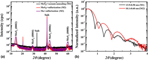
Several structure–property relationships are reported in large-area MoS2 thin films to understand the effect of sulfur vacancies along with complementary first-principles calculations. X-ray diffraction and reflectivity measurements demonstrated that sputtered MoS2 followed by a high-temperature sulfurization produced sharp film–substrate interface along with high crystalline order. Spectroscopic and transport measurements showed that removal of sulfur vacancies promoted A–B excitons, strong in-plane Raman modes, a sharp increase in dc resistivity, and strong photo-conducting behavior. We have clearly demonstrated that a hybrid method using magnetron sputtering can provide high-quality few-layer transition metal dichalcogenide films.

Type
Research Letters
Copyright
Copyright © Materials Research Society 2018 

Access options

Get access to the full version of this content by using one of the access options below. (Log in options will check for institutional or personal access. Content may require purchase if you do not have access.)

References

1.Manzeli, S., Ovchinnikov, D., Pasquier, D., Yazyev, O., and Kis, A.: 2D transition metal dichalcogenides. Nat. Rev. Mater. 2, 17033 (2017).Google Scholar
2.Novoselov, K.S., Mishchenko, A., Carvalho, A., and Castro Neto, A.H.: 2D materials and van der Waals heterostructures. Science 353, 9439 (2016).Google Scholar
3.Zhao, W., Ghorannevis, Z., Chu, L., Toh, M., Kloc, C., Tan, P.H., and Eda, G.: Evolution of electronic structure in atomically thin sheets of WS2 and WSe2. ACS Nano 7, 791 (2013).Google Scholar
4.Ross, J.S., Wu, S., Yu, H., Ghimire, N.J., Jones, A.M., Aivazian, G., Yan, J., Mandrus, D.G., Xiao, D., Yao, W., and Xu, X.: Electrical control of neutral and charged excitons in a monolayer semiconductor. Nat. Commun. 4, 2498 (2013).Google Scholar
5.Lee, Y.H., Zhang, X.Q., Zhang, W., Chang, M.T., Lin, C.T., Chang, K.D., Yu, Y.C., Wang, J.T., Chang, C.S., Li, L.J., and Lin, T.W.: Synthesis of large-area MoS2 atomic layers with chemical vapor deposition. Adv. Mater. 24, 2320 (2012).Google Scholar
6.Geim, A.K. and Novoselov, K.S.: The rise of graphene. Nat. Mater. 6, 183 (2007).Google Scholar
7.Liu, N., Kim, P., Kim, J.H., Ye, J.H., Kim, S., and Lee, C.J.: Large-area atomically thin MoS2 nanosheets prepared using electrochemical exfoliation. ACS Nano 8, 6902 (2014).Google Scholar
8.Radisavljevic, B. and Kis, A.: Mobility engineering and a metal–insulator transition in monolayer MoS2. Nat. Mater. 12, 815 (2013).Google Scholar
9.Gabor, Z.M., Peto, J., Dobrik, G., Hwang, C., Biro, L.P., and Tapaszto, L.: Exfoliation of large-area transition metal chalcogenide single layers. Sci. Rep. 5, 14714 (2015).Google Scholar
10.Dumcenco, D., Ovchinnikov, D., Sanchez, O.L., Gillet, P., Alexander, D.T.L., Lazar, S., Radenovic, A., and Kis, A.: Large-area MoS2 grown using H2S as the sulphur source. 2D Mater. 2, 044005 (2015).Google Scholar
11.Najmaei, S., Liu, Z., Zhou, W., Zou, X., Shi, G., Lei, S., Yakobson, B.I., Idrobo, J.C., Ajayan, P.M., and Lou, J.: Vapour phase growth and grain boundary structure of molybdenum disulphide atomic layers. Nat. Mater. 12, 754 (2013).Google Scholar
12.Yu, Y., Li, C., Liu, Y., Su, L., Zhang, Y., and Cao, L.: Controlled scalable synthesis of uniform, high-quality monolayer and few-layer MoS2 films. Sci. Rep. 3, 1866 (2013).Google Scholar
13.Li, X. and Zhu, H.: Two-dimensional MoS2: properties, preparation, and applications. J. Materiomics 1, 33 (2015).Google Scholar
14.Kang, K., Xie, S., Huang, L., Han, Y., Huang, P.Y., Mak, K.F., Kim, C.J., Muller, D., and Park, J.: High-mobility-three-atom-thick semiconducting films with wafer-scale homogeneity. Nature 520, 656 (2015).Google Scholar
15.Tan, L.K., Liu, B., Teng, J.H., Guo, S., Low, H.Y., and Loh, K.P.: Atomic layer deposition of a MoS2 film. Nanoscale 6, 10584 (2014).Google Scholar
16.Liu, K.K., Zhang, W., Lee, Y.H., Lin, Y.C., Chang, M.T., Su, C.Y., Chang, C.S., Li, H., Shi, Y., Zhang, H., Lai, C.S., and Li, L.J.: Growth of large-area and highly crystalline MoS2 thin layers on insulating substrates. Nano Lett. 12, 1538 (2012).Google Scholar
17.Serna, M.I., Yoo, S.H., Moreno, S., Xi, Y., Oviedo, J.P., Choi, H., Alshareef, H.N., Kim, M.J., Minary-Jolandan, M., and Quevedo-Lopez, M.A.: Large-area deposition of MoS2 by pulsed laser deposition with in situ thickness control. ACS Nano 10, 6054 (2016).Google Scholar
18.Fu, D., Zhao, X., Zhang, Y.Y., Li, L., Xu, H., Jang, A.R., Yoon, S.I., Song, P., Poh, S.M., Ren, T., Ding, Z., Fu, W., Shin, T.J., Shin, H.S., Pantelides, S.T., Zhou, W., and Loh, K.P.: Molecular beam epitaxy of highly crystalline monolayer molybdenum disulfide on hexagonal boron nitride. J. Am. Chem. Soc. 139, 9392 (2017).Google Scholar
19.Tao, J., Chai, J., Lu, X., Wong, L.M., Wong, T.I., Pan, J., Xiong, Q., Chi, D., and Wang, S.: Growth of waferscale MoS2 monolayer by magnetron sputtering. Nanoscale 7, 2497 (2015).Google Scholar
20.Samassekou, H., Alkabsh, A., Wasala, M., Eaton, M., Walber, A., Walker, A., Pitkänen, O., Kordas, K., Talapatra, S., Jayasekera, T., and Mazumdar, D.: Viable route towards large-area two dimensional MoS2 using magnetron sputtering. 2D Mater. 4, 021002 (2017).Google Scholar
21.Wasala, M., Zhang, J., Ghosh, S., Muchharla, B., Malecek, R., Mazumdar, D., Samassekou, H., Gather-Ganim, M., Morrison, A., Lopez, N.P., Carozo, V., Lin, Z., Terrones, M., and Talapatra, S.: Effect of underlying boron nitride thickness on photocurrent response in molybdenum disulfide - boron nitride heterostructures. J. Mater. Res. 31, 893 (2016).Google Scholar
22.Towns, J., Cockerill, T., Dahan, M., Foster, I., Gaither, K., Grimshaw, A., Hazlewood, V., Lathrop, S., Lifka, D., Peterson, G.D., Roskies, R., Scott, R.J., and Wilkins-Diehr, N.: XSEDE: accelerating scientific discovery. Comput. Mater. Sci. 16, 62 (2014).Google Scholar
23.Blaha, P., Schwarz, K., Madsen, G.H., Kvasnicka, D., and Luitz, D.: WIEN2k, an Augmented Plane Wave + Local Orbitals Program for Calculating Crystal Properties (Vienna: Technische Universität Wien, 2001).Google Scholar
24.Pedrew, J. P., Burke, S., and Ernzehof, M.: Generalized gradient approximation made simple. Phys. Rev. Lett. 77, 3865 (1996).Google Scholar
25.Grimme, S., Antony, J., Ehrlich, S., and Krieg, H.: A consistent and accurate ab initio parametrization of density functional dispersion correction (DFT-D) for the 94 elements H-Pu. J. Chem. Phys. 132, 154104 (2010).Google Scholar
26.Mak, K.F., Lee, C., Hone, J., Shan, J., and Heinz, T.F.: Atomically thin MoS2: a new direct-gap semiconductor. Phys. Rev. Lett. 105, 136805 (2010).Google Scholar
27.Padilha, J.E., Peelaers, H., Janotti, A., and Van de Walle, C.G.: Nature and evolution of the band-edge states in MoS2: From monolayer to bulk. Phys. Rev. B 90, 205420 (2014).Google Scholar
28.Lanzillo, N., Birdwell, A., Amani, M., Crowne, F., Shah, P., Najmaei, S., Liu, Z., Ajayan, P., Lou, J., Dubey, M., Nayak, S., and O'Regan, T.: Temperature-dependent phonon shifts in monolayer MoS2. Appl. Phys. Lett. 103, 093102 (2013).Google Scholar
29.Nazir, G., Khan, M. F., Lermolenko, V. M., and Eom, J.: Two- and four-probe field-effect and Hall mobilities in transition metal dichalcogenide fieldeffect transistors. RSC Adv. 6, 60787 (2016).Google Scholar
30.Bhattacharyya, S. and Singh, A. K.: Semiconductor-metal transition in semiconducting bilayer sheets of transition-metal dichalcogenides. Phys. Rev. B 86, 075454 (2012).Google Scholar
Supplementary material: File

Samassekou et al. supplementary material

Samassekou et al. supplementary material 1

Download Samassekou et al. supplementary material(File)
File 2.3 MB