

Digital information can be stored in magnetic, optical, or semiconductor devices. Although significant breakthroughs have occurred in the development of semiconductor-based memories in the last few decades, further increases in storage density and further miniaturization of memory cells are needed for improved performance. Silicon nanowires (Si NWs), due to their large surface-to-volume ratio and high crystallinity, are a promising candidate for miniaturized memory structures.
However, the high growth temperatures and low trapped charge density limits the development of Si NWs-based electronic devices. A research group has now introduced a new approach to build a two-terminal nonvolatile (2TNV) memory, a device that utilizes a varying internal electric field between two electrodes to define memory states, using a low temperature Ga-assisted growth and silicon nitride dielectric layer deposition. The device developed by the group exhibits electrical bistability and read-write-erase states under various applied electric potentials.
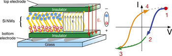
Illustration of schematic two-terminal nonvolatile device (2TNV) with Si nanowires (NWs) as a charge-storage medium in the READ process with applied electrical field Eo and internal electric field Ei in the opposite direction. The current–voltage hysteresis plot explains the working principle of the 2TNV memory. Credit: Scientific Reports.
As reported in a recent issue of Scientific Reports (doi:10.1038/srep27506), the research team, led by Shashi Paul in the Emerging Technologies Research Centre at De Montfort University, fabricated Si NW memories with enhanced charging properties to improve memory storage and a low temperature growth method to reduce the device cost.
The Si NWs in the study were grown on a glass slide sandwiched between a silicon nitride dielectric layer and aluminum metal electrodes. Electrical measurements indicate bistable memory states at 0 and 1 under various applied voltages. The research team built a metal-insulator-semiconductor structure to study the charging effects. The results showed large hysteresis due to the enhanced Si NWs charge-storage capacity and long charge retention time.
“The fabrication method [developed] allows controlled growth of silicon nanowires directly on various substrates through the use of an evaporated catalytic layer,” Paul says. “This extends the use of nanowires for Si-based engineering, science, and the possibilities for a broad range of applications with bottom-up manufacturing.”
“It is exciting that well-aligned silicon nanowires in nonvolatile devices could increase the switching current and improve the electrical bistability,” says Sheng Xu, an assistant professor in the Department of Nanoengineering at the University of California, San Diego, with expertise in the field of nanowire devices. “In addition, these silicon nanowires were fabricated at a low temperature, which holds great implications for scaling up.”
