


As the world came to a standstill in the grip of a pandemic, society's reliance on digital technologies became more apparent than ever. Millions connected to live meetings from home, schools went to online platforms, and video streaming soared. The energy use of cars, airplanes, and office buildings might have plummeted, yet that of server farms skyrocketed.
Data centers are notoriously energy-intensive, consuming 10 to 50 times the energy per floor space of a typical commercial office building, according to the US Department of Energy. Today, they account for about 1% of the world's electrical energy use. But as Internet and personal device use grows, the energy use and emissions of the information and communications technologies (ICT) industry could explode. The future is uncertain, but in one worst-case modeled scenario, ICT could gobble up more than 20% of global electricity by 2030, with data centers using more than a third of that.
Shrinking silicon transistors and packing them more densely on chips has led to faster, cheaper, and more powerful computing. These high-performance chips are also power-hungry. New materials technologies could enable devices and memory that use less energy (see the Energy Quarterly section in the March 2020 issue of MRS Bulletin, doi.org/10.1557/mrs.2020.70).
But high-power computing creates another set of challenges. One is the generation of blistering temperatures that require energy-consuming cooling techniques. The other is the immense energy cost to move data around chips via interconnects.
The industry has relied for decades on good old copper for both heat dispersion and interconnects. Copper is hard to beat when it comes to thermal and electrical conductivity. Better materials such as silver and diamond are prohibitively expensive. Now more than ever, there is a need for novel materials to help tackle thermal management and interconnect challenges.
Besides making laptops uncomfortable to use, overheated chips are slow, unreliable, and sap battery life. “Manufacturers literally have to throttle performance so you won't exhaust the battery in a few hours or burn your knee,” said Eric Pop, a professor of electrical engineering and materials science and engineering at Stanford University. And managing heat at the single transistor, chip, and package level can influence cooling needs all the way up to data centers. “Historical data show that something like half the energy consumption of data centers deals with cooling,” said Pop.
For mobile devices, Samsung and others have introduced copper heat pipes that siphon heat away from the hot central processing unit (CPU). Water in the copper pipe evaporates near the hot CPU, the vapor migrates to the opposite end of the pipe where it condenses, and the cycle repeats. Carbon fibers or silicone, both excellent heat-transferring materials, are sometimes used to thermally connect the CPU to the heat pipe. “It's a really cool invention, pun intended,” said Pop. Yet, “in terms of materials, there haven't been innovations in a long time,” he added. “Heatsinks have been made of copper for as long as there have been heatsinks.”
To make transistors smaller, the industry has moved to complex three-dimensional (3D) designs, such as FinFETs and nanosheets. These create more interfaces between materials with different thermal conductivities, impeding heat flow. As our appetite for computing goes up, future chips will likely have multiple layers of logic and memory, “requiring very dense multiple connections,” said Subhasish Mitra, electrical engineering and computer science professor at Stanford University. “Thermal management is already an issue with 2D, and now it's a problem on steroids for 3D architectures.”
Chip packaging adds further heat-managing challenges. In a traditional package, the chip is connected to the substrate with the help of metal solder bumps. An epoxy or other polymer-based underfill material typically fills the gaps between the bumps. The underfill has 100 times lower thermal conductivity than silicon or metal, barricading heat flow. “Like kinks in a hose, low thermal conductivity electric materials are the kinks that affect the heat flowing across the layers,” said Zeki Celik of Broadcom.
On top, a thermal interface material (TIM) connects the chip thermally to the lid, and then another TIM sits between the lid and the heatsink. TIMs are typically greases, gels, metallic solders or foils, or phase-change materials. The interfaces are rough, and the TIMs, in addition to having high thermal conductivity, need to be very conforming so they can fill in all the poorly conducting air gaps. “We need to have a lot of focused research for these thermal interface materials,” said Celik.
Emerging materials with promising thermal properties might help improve heat management in next-generation electronics. One such material is graphene. In 2015, researchers at Rutgers, The State University of New Jersey, found that a few layers of graphene could quickly channel heat away from hot spots on a silicon chip. “Materials like graphene have showed big promise at lab scale,” said Celik.
Many researchers are also looking at high thermal conductivity cubic crystals, such as boron arsenide, boron nitride, aluminum nitride, and gallium nitride. The last two are already used widely in light-emitting diodes. Their thermal conductivity values of 200– 400 W/mK are several times higher than silicon. Meanwhile, two-dimensional (2D) AlN, BN, graphene, and other materials offer the advantage of anisotropy, said Pop. That is, their conductivity is not uniform in every direction, a feature that can be leveraged to channel heat where needed.
By stacking different 2D materials, he and his colleagues made a 10-μm-thick heat shield that insulated just as well as a sheet of glass 100 times thicker. The device, reported in Science in August 2019, contained layers of graphene, molybdenum disulfide, and tungsten disulfide. Each layer is two or three atoms thick, but because the atoms in the different materials vibrate at different frequencies when heated, “energy doesn't want to pass from one layer to another,” said Pop. “We demonstrated that this stack is a better thermal insulator than an air gap of the same thickness.”
An ultrathin thermal barrier around a chip or just at a power-dense hot spot could keep batteries and other parts of the gadget from overheating and malfunctioning. Another option is to store heat in a phase-change material and send it when needed to the battery, so that it performs well in the cold.
To improve the thermal conductivity of conventional TIMs and underfill materials, many researchers have made composites by filling them with nanomaterials such as boron nitride flakes, alumina or silica particles, graphite, carbon nanotubes, and carbon nanofibers. One challenge with the composites is that while thermal conductivity increases with the fillers, the materials are more viscous and less soft. Their decreased flow makes them harder to use as an underfill that has to flow through the gaps between the solder bumps, and as a TIM that needs to cover all the air gaps on surfaces.
Some have proposed using vertical arrays of carbon nanotubes as TIMs, but this requires more engineering to make the arrays dense and of uniform height. Yet another promising set of materials are 3D foams of high thermal conductivity, such as graphite, metals, or dielectrics like BN or AlN. Filling the pores of these 3D matrices with, say, a phase-change material or thermal grease could boost heat spreading and transfer.
Ideas similarly abound in the area of interconnects. Today's super-dense chips contain meters of copper wiring between transistors. As these interconnects get thinner, resistance goes up, and current can damage them. So chipmakers are looking at a range of suitable materials to replace copper.
Cobalt is one. It has three times higher resistivity than copper, but manufacturers are using it for short connections inside and between transistors. Another option is to wrap copper in graphene. Today's copper wires are protected by a 2-nm-thick layer of tantalum nitride, which is excellent at preventing copper from diffusing, but even that is getting too thick now with transistors shrinking below 5 nm in size.
Zooming out from chips to the system level, reducing the energy use of cooling and transmitting data might require rethinking an industry mainstay, the printed circuit board (PCB), which Celik calls “the weakest link” in heat management. The PCB is made of a fiberglass and epoxy composite, and its purpose is to connect several silicon chips, but this requires the tiny square centimeter chips to be packaged in plastic and placed on the large PCB board, connected to each other by copper tracks and pads. “The packages and PCB are made of a material with two orders of magnitude lower thermal conductivity than metals,” said Celik.
To overcome this problem, University of California, Los Angeles, electrical engineers Puneet Gupta and Subramanian Iyer have proposed getting rid of the packages and the PCB. Instead, all different kinds of chips and electronic components could be directly bonded onto a 500-μm to 1-mm-thick silicon wafer. This means bare chips could be packed closer together and connected with wiring as thin as that on a chip, which would transfer data using less energy. Plus, heatsinks placed on both sides of the thermally conductive silicon wafer could extract more heat.
The semiconductor industry, of course, is not quick to move to new materials and systems. For any novel thermal management and interconnect solution to make the leap from the laboratory into commercial devices will require them to easily integrate into current industry processes.
To this end, in addition to finding better materials, one of the biggest challenges is getting accurate materials data, said Celik. “It was a challenge 20 years ago, and still is a challenge. Most of the time, numbers we get are not accurate or applicable to a numerical simulation environment.” Plus, he added, “At the end of the day, everything becomes a cost issue.”
Materials researchers have already tackled many of these challenges with creative thinking, he said. They now still have an exciting opportunity to make meaningful impacts on the energy use of computing by addressing the pressing thermoelectric and interconnect material challenges.

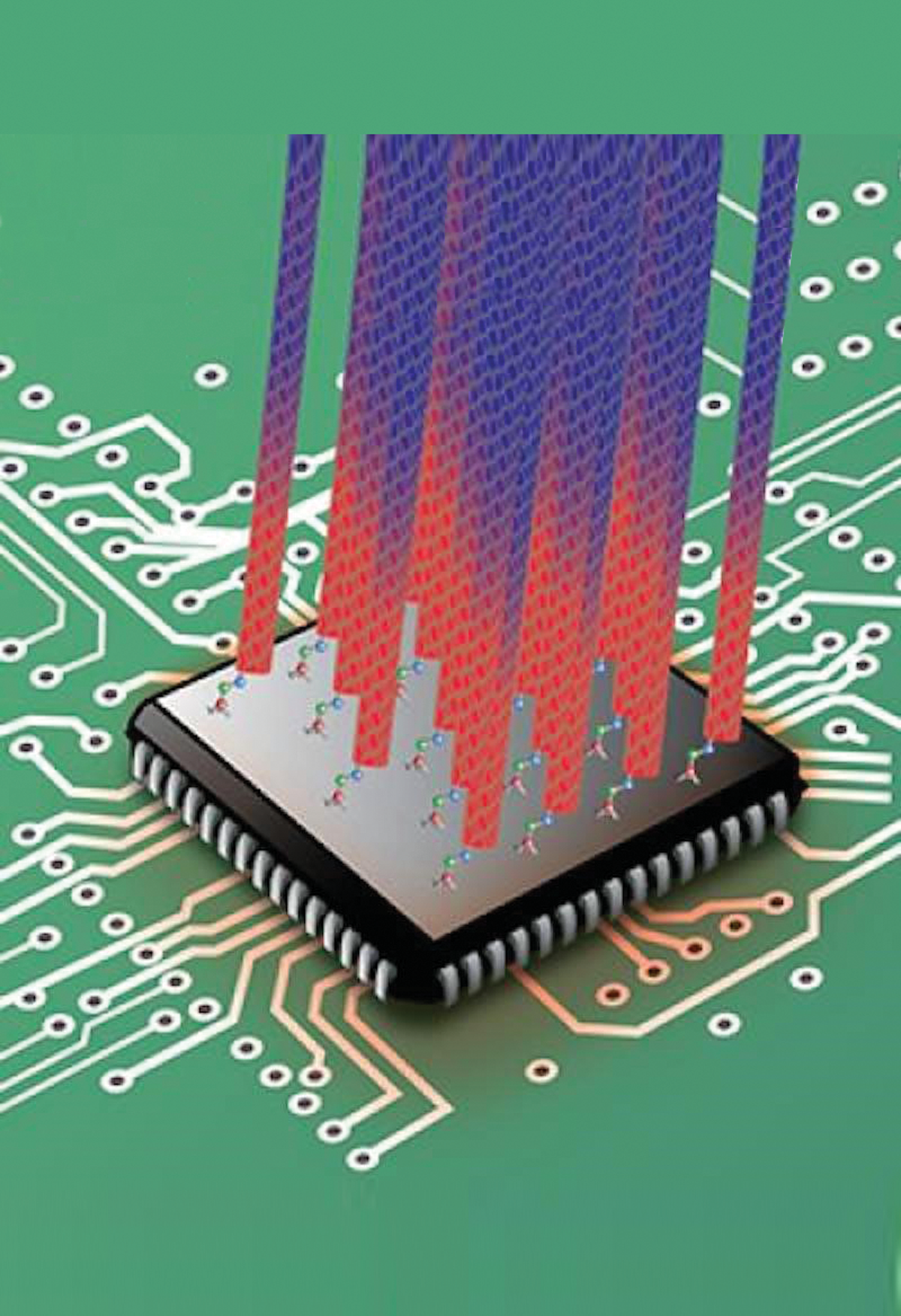
NAMICS has developed high conductive thermal interface materials to meet the demands of today's semiconductor devices. These materials provide heat dissipation for next-generation semiconductor packages. Credit: NAMICS.
