


Introduction
The Merriam-Webster dictionary defines manufacturing as the process of making something from raw materials by hand or machinery, according to an organized plan and with a clear division of labor. Additive manufacturing (AM), an emerging technology, is a subset of the overall manufacturing ecosystem that has the potential to revolutionize the way we both make and consume products. 1 One suggestion made by many casual observers of this technology is that AM will lead to equalization of manufacturing process capability and, thereby, an economically “flat” world, a term coined by Thomas Friedman. Reference Friedman2 Friedman highlights many political–social–technological events as evidence for the leveling of the playing field in economic activities across the world. The ability to design a part and manufacture it anywhere in the world using three-dimensional (3D) printing equipment could be interpreted as the realization of this hypothesis.
Do such predictions about AM represent an achievable reality? For example, we will be able to print a car using AM in the near future. Although this might appear to be science fiction, the startup company Local Motors, in collaboration with Oak Ridge National Laboratory (ORNL), has, in part, demonstrated its feasibility. Local Motors uses an emerging technology, namely big-area additive manufacturing (BAAM), to manufacture the chassis of a small two-seater car that will be powered by an electric power drive. The company Reference Maxey3,4 is striving to implement an open-innovation economic model Reference Chesbrough5 in which every manufacturing step (e.g., design of cars and parts, materials selection, and manufacturing) can be distributed across the world without any barriers.
Based on this example, one might assume that AM has reached maturity for adoption across industrial sectors. However, counterarguments can be made to stress the fact that AM is not advanced; rather, it is clearly an emerging technology with limited applications. 6–Reference Lipson and Kurman8 This article attempts to provide a balanced overview by highlighting the technical challenges and approaches to address this debate. Because AM technology development and deployment are expanding at a rapid pace, this article focuses on a subset of materials considered for industrial deployment, namely, structural materials made up of metals and polymers. Recently, an economic analysis indicated that the adoption of AM for structural applications will require a focused effort on materials specifically developed for AM. 6 Therefore, in this article, we discuss four different challenges to the AM of large metal parts, specifically large-scale manufacturing, in situ process monitoring, computational modeling, and characterization of internal stresses. For each topic, we first define the issue and then describe approaches to solutions, demonstrations of the approach, capabilities, and future prospects. (See the article in this issue by Bandyopadhyay et al., as well as the February 2015 issue of MRS Bulletin, for information about 3D printing of biomaterials.)
Large-scale additive manufacturing technology
Conventional AM processes have three fundamental limitations: Reference Gibson7,Reference Brajlih, Valentan, Balic and Drstvensek9 (1) AM processes build components at a rate of less than 30 cm3/min. (2) The parts are small (<1000 cm3 in volume). (3) The material feedstock is expensive (USD$100/kg). Even with these limitations, polymer and metal AM technologies, in particular, are transforming the biomedical devices and aerospace industries, respectively, by focusing on functional and complex components. However, significant improvements in speed, size, and cost, without the need for an environmental chamber, are likely to open up new applications in other industries.
Approach
In one effort to address these limitations, ORNL researchers developed the BAAM methodology. This technology was demonstrated for 3D printing of plastic components. Reference Holshouser, Newell, Palas, Duty, Love, Kunc, Lind, Lloyd, Rowe, Dehoff, Peter and Blue10 First, low-cost pellets of acrylonitrile butadiene styrene (ABS) were used instead of high-cost preprocessed polymer filaments. Pellet costs are very low, ranging from under USD$3/lb. (USD$1.40/kg) for carbon-fiber- (CF-) reinforced ABS to USD$25/lb. (US$11/kg) for CF-reinforced ULTEM (a polyetherimide resin). Second, rather than extruding a filament through a small nozzle (250 µm), a single-screw extruder was used to melt the ABS pellets and disperse them through a 5-mm nozzle, increasing the flow rate to over 16,000 cm3/min.
Use of the larger nozzle also advantageously changed the thermal behavior of the plastic. Specifically, conventional fused deposition modeling (FDM) systems go from the melt temperature in the extruder to the oven or room temperature in approximately 250 ms. The larger bead decreases the relative surface area of the extrusion, keeping the material warmer for many seconds, thereby allowing for cross-linking between successively deposited layers. The extruder was integrated with a gantry-style robotic automation cell for printing large-scale 3D structures (see Figure 1a).
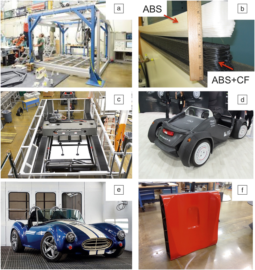
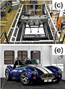
Figure 1. Development stages of big-area additive manufacturing (BAAM). (a) Gantry-style robotic automation system, without any heating environment, was developed and integrated with a single-screw extrusion nozzle. (b) Initial material trials led to extensive distortion with acrylonitrile butadiene styrene (ABS) pellets, whereas use of pellets with ABS and carbon fiber (CF) reduced the distortion. (c) Aerial view of the industrial-scale BAAM system developed by Local Motors. (d) The industrial-scale system was verified by printing out a chassis of a small car, which was then integrated with an electric drive train. (e) The same technology was coupled with traditional manufacturing to produce a prototype similar to the Ford Shelby Cobra, which was also powered by an electric drive train. (f) The same technology has also been used to make molds for use in prototyping during traditional metal-forming processes. Reproduced with permission from Reference Reference Holshouser, Newell, Palas, Duty, Love, Kunc, Lind, Lloyd, Rowe, Dehoff, Peter and Blue10. © 2013 ASM International.
Initial trials of this extruder-based BAAM with ABS material showed extensive warping (see Figure 1b). Interestingly, the use of carbon fiber in the pellets not only increased the strength and stiffness, but also reduced the warping tendency (see Figure 1b). With these key processing and material changes, room-temperature AM with no size constraints and significant reduction in energy intensity was demonstrated. Local Motors has adapted this BAAM technology for industrial scale-up 11 (see Figure 1c).
Demonstration
BAAM technology has been used for two applications: prototype vehicles and molds for sheet metal forming (see Figure 1d–f). For the production of two types of prototype vehicles, one goal was to reduce the number of parts. Most traditional vehicles are assembled with more than 20,000 parts. Through BAAM technology, the newly designed Strati was manufactured with just 50 parts. The design was based on a unified body and frame that weighed approximately 600 kg and required approximately 44 h to manufacture (see Figure 1d).The second demonstration focused on lightweighting, surface finish, and energy absorption. The Cobra, based on a classic sports car, had approximately 200 kg of printed material and took approximately 24 h to print. The design employed a printed frame that provides the load-bearing features of the vehicle integrated with single-wall skins for aesthetics (see Figure 1e). Furthermore, surface finishing techniques based on gelcoat were used to provide a glossy, class-A automotive finish (i.e., free-form surfaces of high quality without imperfections).
Both of these demonstrations exhibit the flexibility and productivity of BAAM technology, at least for the prototyping of automotive vehicles. However, to have a larger impact on the manufacturing industry, this methodology needs to be extended to tooling 6 for traditional manufacturing processes. For example, traditional molds for shaping metal and composite structures take months to manufacture and cost in excess of US$100,000. BAAM enables very rapid, low-cost tool prototyping and low-volume manufacturing. The mold shown in Figure 1f required approximately 8 h to manufacture at a cost of less than $1,000.
Outlook
In 2011, AM sales were valued at USD$1.9 billion, with projections of USD$7.5 billion per year by 2020. However, the industry could exceed USD$100 billion per year if fundamental barriers such as cost, quality, range of materials, and size limitations could be overcome. 12 Specific goals are a factor of 4–10 increase in deposition rate, lower material costs, and closed-loop control to reduce process variations. Reference Frazier13
Current commercial efforts are focused on biomedical and aerospace applications, where speed and cost are not considered as prohibitive as in other industries. To affect a broader range of industries, future efforts should be directed toward extending BAAM to metals. The target requirements include (1) deposition rates exceeding 1000 in.3/h (0.015 m3/h), (2) physical sizes exceeding 500 ft Reference Maxey3 (15 m3), (3) low-cost material feedstocks (USD$1–25/lb. (USD$2–55/kg)), and (4) performance superior to that of parts made by traditional manufacturing. Although some preliminary work based on arc welding, Reference Wang, Williams, Colegrove and Antonysamy14,Reference Ding, Colegrove, Mehnen, Ganguly, Sequeira Almeida, Wang and Williams15 plasma, Reference Martina, Mehnen, Williams, Colegrove and Wang16 laser, Reference Brandl, Baufeld, Leyens and Gault17 and electron beam Reference Taminger18,Reference Brice and Hofmeister19 techniques has been done to scale up the process, these approaches have not reached the targets of displacing large forgings and extrusions typically used in earth-moving equipment, buses, trucks, bridges, and infrastructure.
In situ process monitoring and microstructure control
The ability of AM to fabricate geometrically optimized complex components at significantly reduced costs Reference Dehoff, Duty, Peter, Yamamoto, Chen, Blue and Tallman20 and lead times has been demonstrated. However, generic process and component certification methodologies have not been deployed. As a result, most AM development follows trial-and-error manufacturing and testing, which defeats the potential advantages of AM discussed earlier. Therefore, these disadvantages are being addressed through in situ process monitoring methodologies, many of them originally developed for welding.
Approach
Popular approaches Reference Tapia and Elwany21 to in situ monitoring include tracking spatial and temporal surface variations through optical techniques Reference Clijsters, Craeghs, Buls, Kempen and Kruth22 and temperature measurements using one- or two-dimensional (2D) pyrometers and thermocouples and displacement sensors. Reference Foster, Taber, Babu and Daehn23 Here, we highlight two methodologies for inspecting and monitoring the electron beam melting (EBM) powder-bed manufacturing process.
The first method collects a still image of the surface upon the completion of each layer. Both conventional charge-coupled device and near-infrared images are captured. Image analysis is applied to the thousands of 2D images obtained to yield 3D porosity maps of the component. The resulting 3D images have been compared with 3D x-ray tomography data and were found to show a good correlation. This approach also provides accurate geometrical information on each layer during the build process. In addition, it is a low-cost method for validating as-built component quality and therefore allows for rapid deployment.
The second technique uses both high-speed infrared imaging and optical imaging to track the deposition process under in situ EBM conditions. The resulting images allow for prediction of the surface temperature during the deposition process and estimation of the temperature gradient (dT/dx) and liquid–solid interface velocity (dx/dt). These data can be used to understand the influence of processing parameters (e.g., scanning strategies) on the quality and microstructure of additively manufactured components. Furthermore, process parameters can be specified a priori to achieve spatial control of crystallographic texture in the AM of metallic materials.
Demonstration
An example of high-speed infrared imaging is shown in Figure 2a–b for the deposition of two rectangular blocks. The red boxes in Figure 2a indicate the first layer deposited on an overhanging geometry and show the formation of porosity, which is independent of the focus offset (FO) (the electron beam machine setting describing the displacement of the beam focus). Figure 2b shows an image of the identical regions of interest but after the deposition of two subsequent layers. The variation in porosity here is due to the two different FO values used for deposition: FO = 3 for the block on the left, and FO = 15 for the block on the right. This demonstrates that the FO value is extremely important for controlling porosity in EBM processing.
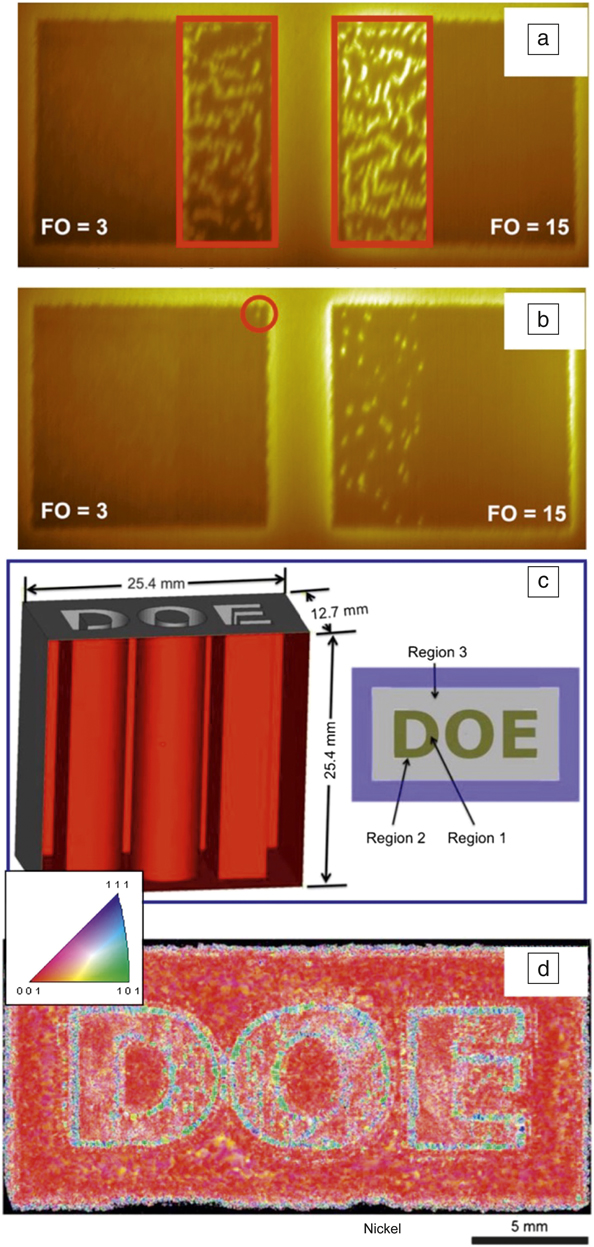
Figure 2. Example of in situ high-speed infrared imaging of electron beam melting using different values of the focus offset (FO = 3 and 15) on an overhang geometry. (a) Image from the first layer, showing the formation of bright spots indicative of porosity. Squares are one inch on a side. (b) Image from the third layer of the same region, showing the reduction of porosity. (c) Demonstration of crystallographic texture control to outline the letters “D,” “O,” and “E,” using a priori design of process control through modifications of electron-beam scans in regions 1 (inside “D” and “O”), 2 (letter bodies), and 3 (outside). (d) Electron backscatter diffraction image of the cross section of the sample processed according to the scan strategy in (c) showing the formation of highly aligned {001} crystal growth and a transition to equiaxed or misoriented growth in the locations outlining the letters. The inset shows the crystallographic color key for the image in (d). Reproduced with permission from Reference Reference Dehoff, Kirka, Sames, Bilheux, Tremsin, Lowe and Babu24. © 2015 Maney Publishing.
In addition to detecting porosity, this analysis allowed for a comprehensive understanding of both solidification and precipitation kinetics. Reference Sames, Unocic, Dehoff, Lolla and Babu25 This understanding leads, in turn, to a fundamental question: Is it possible to control the crystallographic textures in site-specific regions within a component? Conventional EBM scan strategies and process parameters result in coarse columnar grains aligned parallel to the build direction, similar to what is observed in a directionally solidified microstructure. Interestingly, this behavior is prevalent across many alloy systems, including steels and titanium- and nickel-based alloys. Reference Frazier13,Reference Tian, McAllister, Colijn, Mills, Farson, Nordin and Babu26 However, this phenomenon can be rationalized based on directional growth after epitaxial solidification on a preexisting substrate. Reference David and Vitek27,Reference Gaumann, Bezencon, Canalis and Kurz28 Through variations in the process parameters such as beam power, beam velocity, beam focus, and scan strategy, the behavior of the electron beam can be manipulated from that of a line source to that of a point source, which, in turn, can modify the temperature gradient and liquid–solid interface velocity. For example, researchers have demonstrated the ability to control the crystallographic texture in nickel-based superalloys using novel scan strategies (see Figure 2c–d). These strategies were developed using well-understood weld solidification theories Reference Vitek29,Reference Babu, David, Park and Vitek30 and knowledge gained from in situ process sensing and thermal models. Reference Dehoff, Kirka, Sames, Bilheux, Tremsin, Lowe and Babu24,Reference Dehoff, Kirka, List, Unocic and Sames31
Outlook
This demonstration provides a unique pathway for the future design of additively manufactured high-performance metallic components. For example, fatigue crack growth in single-crystal nickel-based alloys is very sensitive to the orientation of the crystals relative to the loading axis. Reference Reed, Wu and Sinclair32 By using the methodology outlined in this section, one might be able to optimize the crystal orientation within a component to achieve site-specific properties and manipulate crack growth characteristics. However, this might not be realized in complex geometries by in situ process monitoring alone. This is partly due to the inability of in situ process monitoring tools to track repeated thermal cycles with heating and cooling rates above 104 K/s. Consequently, there is a need for integrated computational process-modeling tools. Reference King, Anderson, Ferencz, Hodge, Kamath and Khairallah33,Reference Chaudhary, Furrer and Semiatin34
High-performance computational modeling
In AM, materials in their basic form (such as powders, wires, and tapes) are transformed into a finished part through manipulation using different energy sources. These energy sources, including electrons, photons, plasmas, and phonons, interact with the materials, leading to localized diffusion, melting, and high-strain-rate deformation to consolidate them. Reference Gibson7,Reference Hu and Kovacevic35–Reference Yan and Gu43 These interactions are often complex and might not yield the expected target properties. Reference Shen and Chou44 As a result, AM practitioners use trial-and-error optimization exercises similar to those employed in traditional manufacturing. However, the number of variables required to specify the conditions at each position in electron-beam AM, for example, can reach more than 104 (and even higher upon inclusion of a scan strategy) for a given part, rendering attempts at optimization futile.
Approach
To address this challenge, high-performance computing (HPC) tools are being developed to deal with unique features, including (1) localized melting with heat transfer in granular powder media, Reference Korner, Bauereib and Attar45 (2) heat and mass transfer with steep temperature gradients Reference Manvatkar, De and DebRoy46 and high liquid–solid interface velocities, Reference Manvatkar, De and DebRoy47 (3) microstructure evolution, Reference Babu48 and (4) thermomechanics. Reference Denlinger, Irwin and Michaleris49 Here, as a representative example, we describe the use of HPC simulations of heat and mass transfer for predicting the spatial and temporal variation of the melt-pool shape during electron-beam AM of Ti-6Al-4V alloys.
These simulations were performed using the Truchas code from Los Alamos National Laboratory Reference Korzekwa50 with appropriate user routines for path specification. The simulation model in Truchas is a finite-volume code based on continuum conservation equations for mass, momentum, and energy. Reference Fan, Liou and Nurul Amin51,Reference Ferziger and Perić52 The interdendritic liquid metal flow in the mushy zone can be modeled as a Newtonian flow in permeable media. The continuum properties, such as density, velocity, enthalpy, and thermal conductivity, are volume-weighted averages of the properties of the phase constituents. The model includes surface tension, and tracking of the free surfaces is based on the volume-of-fluid method. Reference Francois, Sicilian and Kothe53
Demonstration
Antonysamy experimentally studied the effects of spatial variation in melt-pool shape on the Ti-6Al-4V electron-beam powder melting process. Reference Antonysamy54 The temperature dependence of thermophysical properties has a dominant effect on simulations, emphasizing the importance of coupling the momentum equations with the energy equation, which, in turn, gives rise to strong nonlinearity of the conservation equations. Reference Kruth, Levy, Klocke and Childs55 Truchas implements fully implicit Newton-based solvers to address the strong nonlinear interactions between the various phases and the governing physics. Reference Korzekwa50
Sample results of simulations exploring the role of path sequence in the melting and solidification of Ti-6Al-4V powder are shown in Figure 3 . Reference Babu56 In these simulations, the paths of the electron beam were explicitly tracked, for example, the Hilbert, oxen, and spiral paths shown in Figure 3. The images shown in this figure were extracted from the simulations at given times. (See the supplementary videos that appear at http://dx.doi.org/10.1557/mrs.2015.234.) The results show that the oxen path leads to an oval-shaped melt pool and higher temperature gradients, because there is a significant time delay between subsequent paths within an observation region. In contrast, the Hilbert sequence reduces this time delay and leads to more uniform heating, with circular melt pools with reduced gradients. Similarly, the spiral path leads to spatially varying melt-pool shapes as the beam spirals away from the center to the periphery of the melt-pool volume.
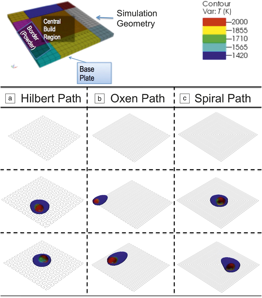
Figure 3. Summary of a high-performance computational simulation of the thermal distribution during electron beam powder processing of Ti-6Al-4V alloy using standard electron-beam current and speed conditions with different scanning strategies at two sequential, arbitrary times. (a) Hilbert path: This ideal space-filling strategy leads to a more oval-shaped melt-pool shape. (b) Oxen path: This is the most common scanning strategy used by most AM machines and leads to elongated ellipsoidal-shaped melt pools similar to those encountered in welding. (c) Spiral path: As this path begins from the center, it results in a more oval-shaped melt pool that evolves into a complex shape with progress in time. Reference Babu56
These simulations provide valuable insight into possible changes in temperature gradients and liquid–solid interface velocities as the melt pool solidifies at different locations. It is interesting to note the differences between these results and welding-process simulation results, where one assumes a constant steady-state melt-pool shape. Reference Gaumann, Bezencon, Canalis and Kurz28 The results also provide confidence that these simulations can be extended to other alloy systems to obtain site-specific crystallographic texture, as discussed in the previous section.
Outlook
For rapid optimization, detailed heat- and mass-transfer simulations need to arrive at a simplified form of the thermal loads, which, in turn, can use coarse-grained thermomechanical models. Reference Prabhakar, Sames, Dehoff and Babu57 The models allow for the prediction of the residual stress and distortion. These coarse-grained simulations need not resolve the actual path of the electron beam. Such a methodology is often used in integrated process modeling of welding. Reference Babu, Furrer and Semiatin58,Reference Goldak and Akhlaghi59 Furthermore, these models need to be verified and validated 60 with ex situ characterization tools, including neutron diffraction instruments. Finally, these computational models must be made available to the wider AM community in a simplified on-demand format to allow for rapid process design. For example, a web-based computational weld mechanics tool has already been developed and deployed within industrial organizations. Reference Zhang and Yang61
Evaluation of residual stress in additively manufactured components using neutron scattering
As mentioned earlier, AM technologies allow for the fabrication of complex metallic structures with internal features. To evaluate these interior features, one needs a technique that can probe deep into metallic parts nondestructively. Neutron scattering is ideal because of its ability to penetrate materials to a depth of a few mm. For additively manufactured components, one can use this technique to characterize locked-in residual stresses, Reference Watkins, Bilheux, An, Payzant, Dehoff, Duty, Peter, Blue and Brice62 as well as spatial crystal orientations of grains within the sample. Reference Dehoff, Kirka, Sames, Bilheux, Tremsin, Lowe and Babu24
Approach
Typical neutron sources are either reactor-based or spallation-based. Beamlines at these sources typically, but not exclusively, condition the neutron beams to be monochromatic or polychromatic, respectively, wherein the wavelength is constant and the diffraction angle is scanned or the diffraction angle is held constant and the wavelength is varied. Reference Hutchings, Withers, Holden and Lorentzen63 Components are typically mounted on a goniometer with rotation and xyz translation stages to manipulate the sample as needed with respect to the incident beam and detector(s). The large depth of penetration (or low scattering efficiency) and two source types allow for a wide range of interesting research for AM, particularly for in situ studies.
For studies of residual stress, a gauge volume within the part is selected based on the matrix grain size and the spatial resolution desired. The sample can be mapped by translating it with respect to the beam and detector. Typical results for a neutron residual-stress measurement are series of diffraction patterns from different regions of the component (mapping) or under different conditions (in situ loading, etc.). Reference Hutchings, Withers, Holden and Lorentzen63–Reference Hutchings and Krawitz65
Demonstration
Many AM practitioners hypothesized Reference Cheng and Chou66 that components made by EBM metal-powder-bed AM will have lower residual stress than those produced by direct laser metal sintering (DLMS) because of the lower cooling rates from the processing temperature in EBM. Although this hypothesis has never previously been validated, Sochalski-Kolbus et al. Reference Sochalski-Kolbus, Payzant, Cornwell, Watkins, Babu, Dehoff, Lorenz, Ovchinnikova and Duty67 recently experimentally evaluated it by using neutron scattering (see Figure 4 ).
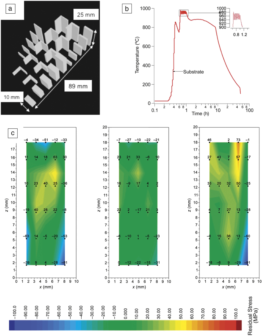
Figure 4. Measurements of residual stresses in a sample made by electron beam melting (EBM) additive manufacturing of metal. (a) Locations of 5 × 10 × 20 mm3 rectangular prisms can be seen among “L”-shaped geometries that were produced using the EBM process. (b) Plot of substrate temperature as a function of time, confirming very slow cooling (>30 h) to room temperature from the processing temperature of approximately 900°C. (c) Measured variations of residual stress in the x, y, and z directions using force and momentum balance. Reproduced with permission from Reference Reference Sochalski-Kolbus, Payzant, Cornwell, Watkins, Babu, Dehoff, Lorenz, Ovchinnikova and Duty67. © 2015 Springer.
Simple rectangular samples were produced in an EBM apparatus made by the Sweden-based company Arcam using powders of the high-strength, corrosion-resistant nickel chromium alloy 718. To simulate practical industrial conditions, these samples were produced in a nested manner with other geometries (see Figure 4a) within a build chamber. During processing, the electron-beam current was varied from 2 mA to 20 mA, and the raster speed was varied from 52 cm/s to 875 cm/s. The substrate temperature varied in the range of 800–900°C during processing and decreased very slowly thereafter (see Figure 4b).
After completion of the geometries shown in Figure 4a, the whole chamber was slowly cooled to room temperature at a rate of 21.68°C/h. The samples were then carefully extracted from the substrate. One of the samples, shown in Figure 4a, was sliced into small pieces to obtain the stress-free lattice parameter (d 0). In another sample, the interplanar spacings, d, of (311) crystallographic planes were measured. Using the series of d values and the strain-free reference value d 0, the strain within the sample along the x, y, and z directions was calculated as ε = (d – d 0)/d 0. Next, using the appropriate elastic constant, the residual stress was determined. The residual-stress maps shown in Figure 4c demonstrate that the stress values in all directions were within a small range from –100 MPa (compressive) to +100 MPa (tensile), confirming the initial hypothesis of the AM community.
These data were also compared with similar sample geometries made by the DLMS process with alloy 718 powders. As expected, in DLMS samples, the residual stresses were higher and varied from –550 MPa to 550 MPa. This large residual stress can be attributed to faster cooling from the processing temperature, because of a lack of preheating, a low laser power, and a reduced layer thickness. It will be of interest to compare the fatigue properties of these samples in future studies, because residual stress distributions affect the spatial and temporal growth of fatigue crack growth. Reference Hwang and Chang68
Outlook
Evaluation of residual stresses within internal features is extremely important for computational-model validation, processing refinement, and component functionality. One future direction is a merger of this technique with the Bragg-edge transmission technique, Reference Santisteban, Edwards, Priesmeyer and Vogel69–Reference Meggers, Priesmeyer, Trela and Dahms72 also called neutron strain tomography. Reference Abbey, Zhang, Vorster and Korsunsky73 For imaging tomography, a series of neutron scattering images are first recorded. These images are corrected, and a 3D representation of the volume is reconstructed using software. Reference Watkins, Bilheux, An, Payzant, Dehoff, Duty, Peter, Blue and Brice62 In this technique, which is now coming to the fore, a portion of a component is typically imaged with a 2D detector at a fixed Bragg angle as the neutron wavelength is varied by either scanning the incident monochromator angle or utilizing a pulsed neutron source. Once the wavelength is sufficiently long, Bragg scattering is no longer possible (2θ > 180°), and the transmission through the sample increases rapidly (i.e., a Bragg edge appears). This occurs for the various crystallographic planes available within the crystal structure of the sample. Because these edges are indicative of the average interplanar spacing, it is possible to calculate the average residual strain/stress in the direction of the transmitted beam.
When appropriate, this technique can collect a large amount of data in a small amount of time compared to traditional neutron residual-strain-mapping techniques with additional neutron tomography data. Furthermore, the diffraction data need to be complemented with detailed microstructural and hardness characterizations in the x–y, y–z, and x–z cross sections. Reference Tian, McAllister, Colijn, Mills, Farson, Nordin and Babu26 Such combined characterizations will likely be the preferred method as detectors and software advance in the future. Comprehensive characterization will be crucial for verification and validation of computational models for AM processes, as well as qualification of mission-critical components.
Summary and conclusions
Recently, an economic analysis was performed to evaluate the competitiveness of AM for structural applications. 6 This analysis suggested the following critical research and development directions for the rapid adoption of AM.
First, technologies must be developed for large-scale and high-productivity AM with low-cost material feedstocks and minimal environmental controls. Potential confirmation of this need was demonstrated through BAAM of polymer composites for automotive prototype and tooling applications.
Second, to minimize trial-and-error AM process design and development, in situ optical and thermal sensing methodologies have been developed and demonstrated. The corresponding measurements can also be used to control thermal gradients and liquid–solid interface velocities to achieve site-specific microstructure control. This was demonstrated for the EBM metal-powder-bed AM of alloy 718 by inducing site-specific columnar and misoriented solidification grain texture throughout the volume of the build.
Third, to induce these site-specific microstructural changes, a priori design of processing parameters has to be carried out without trial-and-error experiments. To meet this need, high-performance computing (HPC) tools based on fundamentals of heat and mass transfer are required. The utility of an HPC tool for evaluating the spatial and temporal variations of Ti-6Al-4V melt-pool shapes during EBM processing with different scan paths was demonstrated.
Finally, with the ability to fabricate complex 3D structures with AM technologies, there is a need to evaluate the locked-in residual stress within features that are buried inside the sample. Comprehensive neutron diffraction measurements of lattice parameters with high spatial resolution provide a pathway to meet this need. This capability was demonstrated by measuring and comparing residual stresses in alloy 718 samples made by EBM AM.
Acknowledgments
Research discussed in this article was sponsored by the US Department of Energy (DOE), Office of Energy Efficiency and Renewable Energy, Advanced Manufacturing Office, under Contract DE-AC05-000R22725 with UT-Battelle, LLC, and by the Laboratory Directed Research and Development Program of Oak Ridge National Laboratory (ORNL), managed by UT-Battelle, LLC. Research at ORNL’s High Flux Isotope Reactor was sponsored by the Scientific User Facilities Division, Office of Basic Energy Sciences (BES), and US DOE. Some of the neutron diffraction characterization was supported by the Division of Chemical Sciences, Geosciences, and Biosciences, Office of BES, US DOE, under Contract DE-AC05-000R22725 with ORNL, managed and operated by UT-Battelle, LLC. The authors thank Drs. Ralph Dinwiddie and Lindsay Kolbus for technical contributions to this work.


