Introduction
What characteristics are common among batteries, butterfly wings, and ferroelectric ceramics? Despite coming from different origins and being explored mostly in non-overlapping areas of scientific inquiry, these materials possess two common characteristics. One is the presence of complex nanoscale structures—from intricate hierarchical assemblies of butterfly wings spanning multiple orders of magnitude in size to random yet tailored structures of battery cathodes to complex nanoscale ordered patterns in relaxor ferroelectrics. The second common characteristic is the presence of electromechanical coupling, that is, mechanical responses to applied electric potentials (biases) and fields (Figure 1). The electromechanical behavior, in turn, is directly related to material functionalities—from diffusion rates and molar volumes in ionic materials to concentrations and orientations of polar bonds in proteins and biomolecules to surface reaction rates in fuel cell materials [Reference Kalinin1].

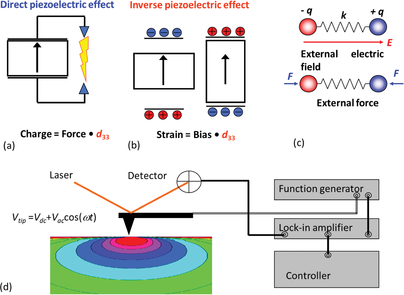
Figure 1: Direct (a) and inverse (b) piezoelectric effect. The application of mechanical stress to materials results in charge separation and generation of bias, whereas application of electric field results in mechanical deformation. In crystals, d33 (the primary value of piezoelectric coefficient tensor defining response in this geometry) ranges from ∼2 pm/V (quartz) to ∼500 pm/V (some compositions of lead zirconate-titanate, PZT). (c) This electromechanical coupling extends to the single polar bond level. (d) Elementary setup for piezoresponse force microscopy measurements based on the lock-in detection of periodic surface deformation induced by electrical bias applied to an SPM tip. In this setup, the SPM probe serves as both the moving electrode and the sensor for bias-induced surface deformation. (a–c) are modified and reproduced with permission from [Reference Kalinin1], Annual Review of Materials Research, vol. 37 © 2007 by Annual Reviews, http://www.annualreviews.org.
Electromechanics
Electromechanics was one of the root areas of modern science. The seminal experiments by Galvani, who demonstrated the contraction of frog legs exposed to a spark of static electricity, and Volta, who invented the first wet-cell battery (at least, the one that was copied afterwards—see “Baghdad battery” on Wikipedia for potential earlier history), laid the foundation to the modern theory of electricity and electrical engineering. These early investigators were the first to study electromechanical coupling in a scientific setting. Yet after that, electromechanics took a long hiatus in emerging as a scientific discipline; it was often considered to be a subset of mechanics dealing with piezoelectric solids or mechanobiology. The reason for this relative dearth of research effort is the extreme smallness of electromechanical coupling coefficients, which for most materials are in the 1–10 pm/V range. In comparison, the radius of the hydrogen atom is 53 pm. In other words, applications of voltages in the “safe” 1–10 V range to a piece of material between two electrodes results in displacements on the order of the size of a hydrogen atom. Secondly, the simplest form of electromechanical coupling—piezoelectricity—is described by the third rank tensor. Consequently, in biological materials and other complex systems the electromechanical properties tend to average to zero. Electromechanics is everywhere, but it tends to manifest on the nanometer scale of individual structural units in complex materials, can average to zero in macroscopic systems, and is small even on the nanoscale. Hence, despite the fact that electromechanics can yield plentiful information on biological, ferroelectric, and electrochemical functionalities, it remained difficult, if not impossible, to explore.
Scanning probe microscopy
The exponential developments of nanoscience and nanotechnology in the last decade of the 20th century were brought about by the emergence of the tools that can visualize, probe, and manipulate matter on the nanometer and atomic level [Reference Gerber and Lang2]. Before the 1980s the main tools for nanoscale visualization were based on electron beam imaging. Subsequently, the efforts of Binnig, Rohrer, and Quate have brought forward the concepts of scanning probe microscopy (SPM), including scanning tunneling microscopy (STM) [Reference Binnig3] and atomic force microscopy (AFM) [Reference Binnig4]. In STM, an atomically sharp probe is used to trace the surface of conductive materials using tunneling tip-surface current to maintain fixed distance between the two. The extreme spatial localization of tunneling current in an atomically defined junction, made way for atomic resolution imaging and spectroscopy in a benchtop instrument. The AFM used the concept of a localized probe interacting with the surface via a pliable cantilever capable of detecting minute atomic-scale forces. This sensitivity was achieved by reflecting a laser beam off the cantilever and detecting shifts in the beam with a sensitive photodiode detector. Surface topography can be measured using feedback to maintain the force between the tip and the surface. In addition, more complex measurement modes involving electrically, chemically, or magnetically sensitized probes enabled corresponding materials functionalities to be explored.
Piezoresponse force microscopy
The advent of SPM has transformed electromechanics from a relatively obscure and poorly accessible aspect of materials science to a wide-open field of experimental exploration. The hallmark of AFM is extreme high sensitivity to vertical displacements, on the order of picometeres (pm), which immediately satisfies one of the key requirements for electromechanical measurements. Secondly, application of an electric bias to the tip in contact with the material surface results in the concentration of electric field in the tip-surface junction area, simply due to the geometry of the system and the dielectric constant mismatch between air (or vacuum) and material. Taken together, these two factors allow for straightforward probing of electromechanical coupling on the nanometer scale, as realized in piezoresponse force microscopy (PFM) (Figure 1d) as popularized by Kolosov and Gruverman [Reference Kolosov5,Reference Gruverman6].
There are two more considerations relevant to PFM. The first is the quantitative nature of the PFM signal. Both simple dimensionality analysis and complex exact theories predict that the tip-induced electromechanical response in a linear piezoelectric material does not depend on the tip-surface contact area. Hence, under a very general set of conditions, the signal measured by the microscope will be representative of the electromechanical properties of material only [Reference Kalinin7]. Secondly, many materials undergo phase transformations or electrochemical processes under the application of a local electric bias. These effects range from polarization switching in ferroelectrics to electrochemical polarization and reactions in ionic materials to complex electrophysiological responses. The combination of these two factors enables a broad range of time- and voltage-spectroscopies to be implemented in PFM [Reference Vasudevan8], providing a window into ferroelectric [Reference Gruverman and Kholkin9], electrochemical [Reference Balke10], and biological [Reference Kalinin11] functionalities of materials.
Lectures on Piezoresponse Force Microscopy
The collection of lectures deposited on the YouTube channel M*N: Microscopy, Machine Learning, and Materials guides the listener though the history of electromechanics to the basic principles of PFM, implementation of PFM in liquids and ultrahigh vacuum, dynamic PFM measurements, and multidimensional PFM spectroscopies. Developed and narrated by the author, and based on multiple presentations and tutorials given over 20 locations worldwide since 2006, these lectures comprise more than 350 slides and 7 hours of presentation.
Lecture 1
The first lecture, “Introduction to piezoresponse force microscopy and spectroscopy,” introduces the listener to the history of electromechanics starting from Galvani and demonstrates the breadth of the systems exhibiting electromechanical coupling—from single crystals of quartz and ferroelectrics to flexoelectricity in graphene and polar chemical bonds in biomolecules (Figure 1). It introduces the basic principles behind PFM and gives multiple examples of PFM imaging of ferroelectric ceramics, biological systems, and electrochemical materials (Figures 2 and 3). It also briefly introduces future opportunities for PFM, notably nanoscale electromechanical systems and molecular electromechanical machines.

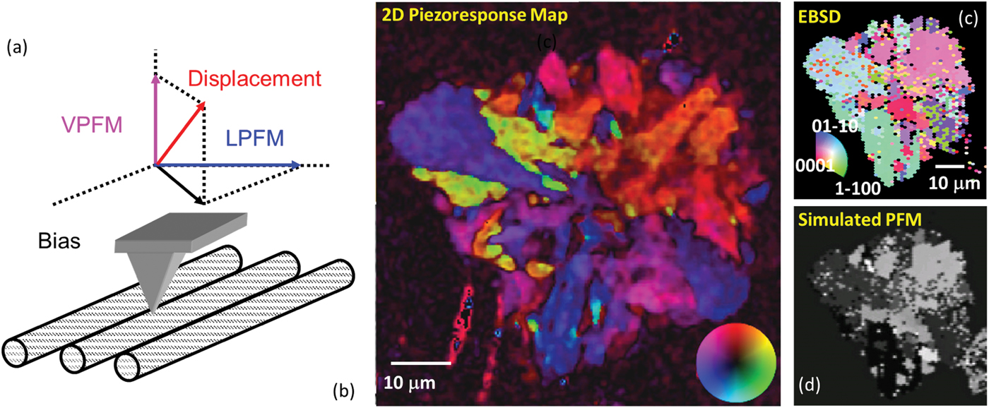
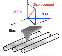
Figure 2: Vector detection in PFM. Detection of vertical and lateral (torsional) components of cantilever deflection allows measurement of two out of three components of the surface deformation tensor. Mechanically rotating the sample by 90 degrees allows the full response vector to be measured. (b) Vector PFM map of the lithium-containing glass ceramics and (c) electron beam selective diffraction image of the same region. (d) Matching the orientation data from EBSD and PFM vector signal allows insight into the piezoelectric tensor properties of a material. Partially adapted and reprinted from [Reference Gupta29] with the permission of AIP Publishing.
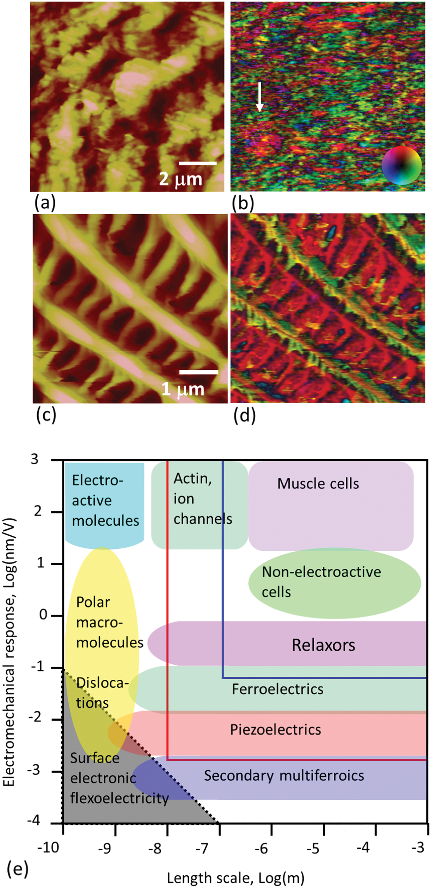
Figure 3: Electromechanical imaging of (a,b) deer antler and (c,d) butterfly wing. Shown are the (a,c) surface topography and (b,d) vector piezoresponse signals. (e) Response and length scale diagram of electromechanical phenomena in biological, macromolecular, and inorganic systems. (a,b) adapted from [Reference Rodriguez30] with permission from Elsevier. (c,d) adapted from [Reference Kalinin11] with permission with permission from Elsevier.
Lecture 2
This lecture, “Contact mechanics and resolution theory,” describes the basic signal formation mechanisms in SPM and shows that PFM is in fact complementary to such techniques as force-sensitive AFM and current-detection methods such as scanning tunneling microscopy (STM). It describes the existing theories for signal formation in PFM, including the extension of classical Hertz contact mechanics toward transversely isotropic piezoelectric and the decoupled model [Reference Felten12,Reference Kalinin13] that allowed approximate analytical solutions for arbitrary material symmetries and domain configurations. The lecture then proceeds to describe resolution theory [Reference Kalinin14] as it is applied to PFM, both from the fundamental theoretical side and in applications for experimental data and image reconstructions.
Lecture 3
In the third lecture, “Dynamic behavior and excitation modes in PFM,” the listener is introduced to the basic principles of dynamic cantilever behaviors. In PFM, and for dynamic AFM methods in general, cantilever resonances are used to amplify pm-scale surface displacements. However, while electromechanical responses of the surface (for linear piezoelectric) are quantitative and do not depend on contact area, the resonance conditions can change because of surface roughness conditions. Hence, the knowledge of the cantilever dynamics is crucial for understanding and mitigating such indirect cross talk. Further, the origins of lateral and longitudinal signals in PFM are discussed [Reference Kalinin15].
An important aspect of PFM is that classical phase-locked loop based resonance tracking methods do not apply in PFM, a consequence of the physical under-determineness of the system. Band excitation (BE) [Reference Jesse16] mode (Figure 4) is introduced as a universal approach for SPM detection that significantly broadens the range of systems explorable by PFM (Figure 3e). In BE, the system is excited, and the response is measured at multiple frequencies at the same time, allowing capture of the segment of the amplitude-frequency spectrum of the cantilever. This BE method is universally applicable in dynamic SPMs, bringing the advantage of parallel detection. Examples of BE imaging and spectroscopy are discussed. Finally, the listener is introduced to the G-Mode SPM, based on full-information capture of the photodiode signal with subsequent physics-based or information-theory-based analysis, allowing for increase of information content in PFM and spectroscopies.
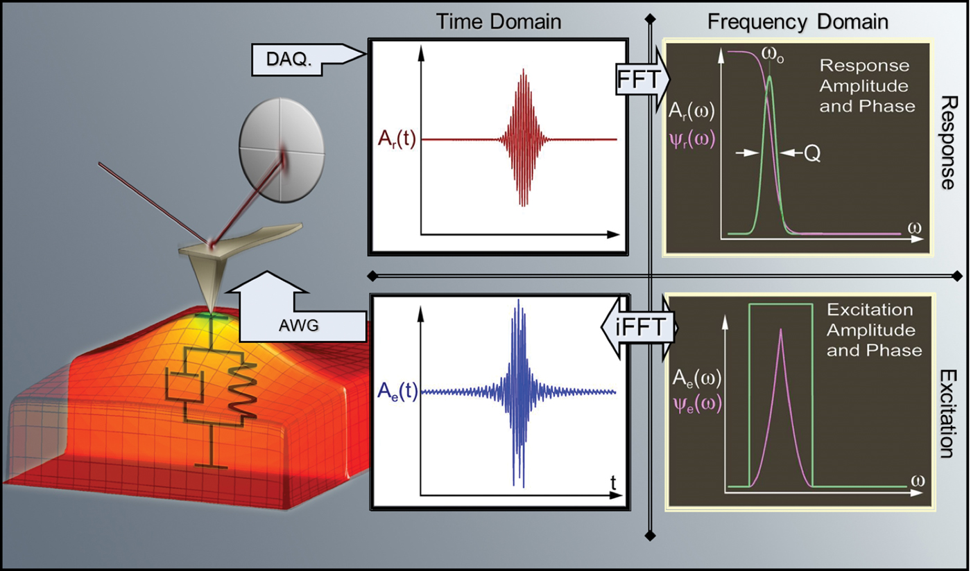
Figure 4: Band excitation method in SPM. Classical single-frequency SPM methods use the excitation and detection via a sinusoidal signal corresponding to single frequency in Fourier space. This approach fundamentally limits the amount of information and quantitativeness of classical SPM methods because the system is fundamentally underdetermined. The band excitation principle introduces parallel excitation and detection methods that enable quantitative resonance-enhanced measurements in PFM, and is broadly applicable to other SPM techniques. Reproduced with permission from [Reference Jesse16].
Lecture 4
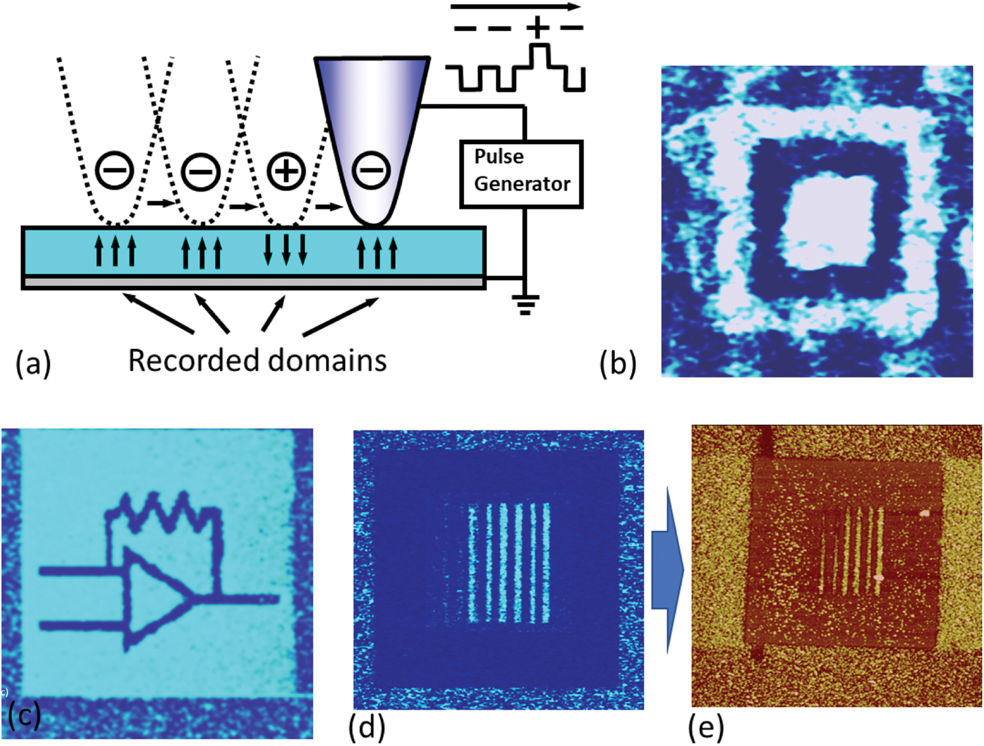
The fourth lecture in the series is “Polarization switching by PFM.” The defining characteristic of a ferroelectric material is that polarization can be switched by the action of an electric field. The size of the individual domains in ferroelectric materials can be extremely small, attracting attention to these materials for ferroelectric non-volatile memories (FeRAM) and data storage. In the context of PFM experiments, polarization can be switched locally by the tip and subsequently visualized in the PFM imaging mode, enabling domain patterning and drawing (Figure 5). These methods can be used for probing and studying domain formation, as well as for exploring stability mechanisms, domain wall dynamics, and other fundamental mechanisms of domain behavior. At the same time, domains with dissimilar polarization orientation have different chemical and photochemical reactivity, enabling ferroelectric lithography of metal oxides capable of sub-100 nm feature sizes. Subsequently, the listener is introduced to polarization switching in multiaxial ferroelectrics and the use of directed tip motion to ensure formation of domains with a prescribed in-plane polarization component [Reference Balke17]. A significant part of the discussion is devoted to the effect of screening processes on polarization switching. Generally, polarization in ferroelectrics is unstable unless the polarization charge is screened by electrodes, near-surface band bending, or adsorption. The latter mechanisms are realized for ferroelectric surfaces in ambient environments. Correspondingly, polarization switching is impossible without the redistribution of screening charges, and the latter can be a major factor controlling the rate and spatial localization of the process. Illustrating this concept, examples of chaotic behavior and complex domain evolution during PFM polarization switching are demonstrated. Finally, the listener is given a brief overview of lateral polarization switching in devices, environmental effects in PFM, and polarization switching in ferroelectric capacitors.

Figure 5: Ferroelectric domain writing and ferroelectric lithography. (a) Application of an electrical bias to the tip during scanning can induce polarization switching in a ferroelectric material that can be further read-out by PFM imaging. Simple figures such as (b) are often used as a proof of ferroelectricity in new materials; see [Reference Vasudevan31] for the discussion of associated issues. Alternatively, the microscope can be configured for patterning more complex domain patterns (c). The variability in chemical and photochemical reactivity between dissimilar domains can be used as a basis for ferroelectric lithograph. Shown here is (d) a PFM pattern and (e) deposited silver nanoparticles following the PFM domain pattern. (d,e) reprinted with permission from [Reference Kalinin32]. Copyright 2004 American Chemical Society.
Lecture 5
The fifth lecture, “Polarization switching spectroscopy in PFM,” introduces the spectroscopic modes in PFM. In its basic implementation, piezoresponse force spectroscopy (PFS), more commonly known as PFM hysteresis loop measurements, is based on the application of a series of square pulses with the triangular envelope to the tip. The “on” state switches polarization in the material, resulting in nucleation and progressive growth of a ferroelectric domain. The PFM response detected in the “off” state allows for the changes in electromechanical response from the detected domain. When plotted as a function of the pulse bias, an electromechanical response exhibits the characteristic hysteresis shape, hence giving rise to the name. The hysteresis loop parameters, such as nucleation and coercive voltage, are directly related to the bias-induced polarization switching mechanisms. The lecture introduces basic principles and multiple examples of PFS, as well as the role of detection parameters on signal. In switching spectroscopy PFM (SS-PFM), the hysteresis loops are measured over the dense grid of analysis points [Reference Jesse18], allowing for the collection of multidimensional data sets containing information on polarization switching across the surface. Implementation and data analysis in PFS are described, as are examples of nucleation mapping in ferroelectrics [Reference Jesse19], and polarization switching at preexisting ferroelastic and ferroelectric domain walls [Reference Aravind20] and bicrystal grain boundaries [Reference Rodriguez21]. These methods thus allow probing of polarization dynamics on single atomically defined defects. The combination of phase field theory and PFM is introduced as a way to get insight into associated mesoscopic mechanisms. Finally, the lecture concludes with a brief foray into neural networks and machine learning to connect PFM signal to statistical physics models.
Lecture 6
This lecture, “Advanced spectroscopic modes in PFM,” synthesizes the concepts in several previous lectures and illustrates how band excitation and G-Mode detection can be combined with the time-spectroscopy and voltage-spectroscopy modes to give rise to 4-D, 5-D, and even 6-D spectroscopies. In this case, the inherently quantitative nature of the BE PFM allows large volumes of high-veracity data to be obtained. Coming to the forefront are the issues of exploratory data analysis of high-dimensional data and its connection to material-specific functionalities. Several examples are illustrated, including Preisach density mapping in disordered ferroelectrics [Reference Bintachitt22], probing elasticity changes during polarization switching [Reference Lindgren23], and probing polarization dynamics in relaxors [Reference Kalinin24].
Lecture 7
The final lecture is “PFM in liquids.” While the majority of PFM studies are performed in ambient and vacuum environments, imaging in liquids presents an obvious interest for probing biological systems or using liquid as an electrode for ferroelectric switching. Yet the practical operation of PFM typically implies large voltages, well outside electrochemical stability windows of most electrolytes. Similarly, cantilever dynamics will be strongly affected by a liquid medium. This lecture introduces the viewer to the elegant and unusual physics of liquid PFM that both makes imaging possible and opens a window into probing the unusual regime of collective phenomena in ferroelectrics [Reference Rodriguez25,Reference Rodriguez26].
Overview
This set of lectures provides an integrated overview of electromechanical measurements on the nanoscale, bringing together multiple concepts from vastly dissimilar areas of scanning probe microscopy, ferroelectricity, electrochemistry, and machine learning. While the level of presentation is necessarily superficial, the references provided allow the viewer to dig deeper into the specific concepts and applications and prepare to start a research effort in this exciting field.
This discussion would be incomplete without mentioning that to date PFM has been developed primarily in the context of ferro- and piezoelectric materials. While applications in biological and electrochemical systems have been demonstrated, the overall volume of research effort in these areas has been limited. Note that the high-field regimes at the tip-surface junction open pathways for probing exotic regimes of electronic and ionic transport and electrochemical reactivity. Such research is rarely, if at all, realizable in macroscopic systems. Similarly, PFM in liquids opens the opportunity for probing electromechanical and electrochemical processes at nanoscale and molecular levels, opening pathways for probing molecular electromechanical machines and other applications. The data analysis and visualization bottlenecks, which stymied the field as recently as two years ago, are now being circumvented via the adoption of big data and machine learning tools [Reference Kalinin27,Reference Kalinin28]. This is an exciting area for exploration and discovery.
Acknowledgments
The work was supported by the Center for Nanophase Materials Sciences, a U.S. Department of Energy, Office of Science User Facility at Oak Ridge National Laboratory.