


Introduction
Seagate Technology, a manufacturer of advanced hard-disc drives (HDDs), uses many microscopy and analytical techniques, including scanning probe microscopy (SPM), scanning electron microscopy (SEM), X-ray photoelectron spectroscopy (XPS), Fourier transform infrared (FT-IR) spectroscopy, Auger electron spectroscopy, and others to identify nanoscale contamination. These techniques vary in sample preparation requirements, chemical specificity, spatial resolution, acquisition and analysis time, complexity, automation capabilities, and cost. Several systems have very high spatial resolution but suffer from inadequate chemical specificity for the determination of organic contamination (Figure 1). Some systems have high chemical sensitivity but have poorer spatial resolution or are slower in time-to-data and require specialized training. For example, traditional FT-IR microscopy methods with spatial resolution >10 μm fail to efficiently characterize submicron contamination and involve sample preparation methods, such as attenuated total reflection (ATR), that do not support automation. State-of-the-art recording head clean rooms and processes are designed to deliver a clean recording head to high-tolerance magnetic recording systems. Contamination identification and control is critical to the ongoing successful development of the manufacturing processes needed to deliver new HDD technologies.
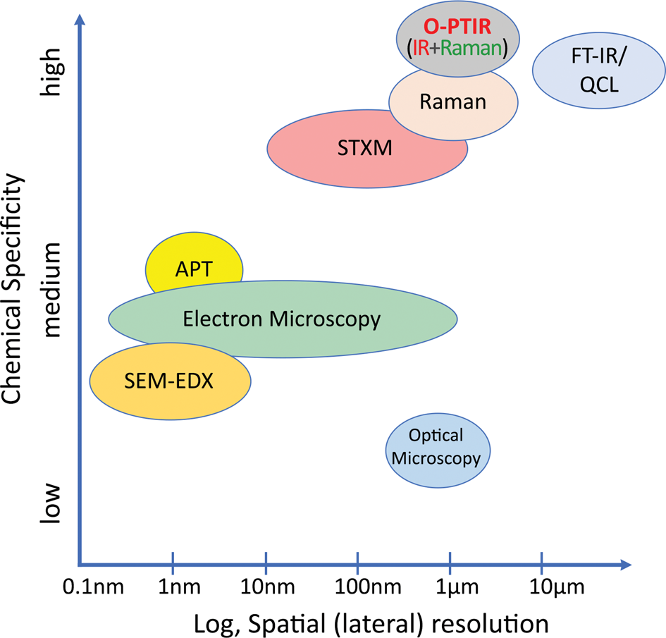
Figure 1: Spatial resolution and relative chemical specificity of correlative methods.
During a recent Seagate Technology review of technology used to identify contamination, a relatively new technique, Optical Photothermal Infrared (O-PTIR) spectroscopy, was evaluated and found to provide a better balance between chemical specificity, spatial resolution, and complexity than other techniques. O-PTIR microscopy, with its submicron capability, limited sample preparation needs, typical microscopy training, and IR spectra that are comparable to spectra collected using current FT-IR methods, was found to be a valuable addition to Seagate's contamination characterization suite. To test the system, a customized sampling accessory was built that allowed loading of multiple samples during one measurement run to improve efficiency and time-to-answers. In a series of recent analyses, more than 90% of the organic contaminates were identified using O-PTIR. In less than one year, a commercial mIRage™ O-PTIR microscope (Photothermal Spectroscopy Corp) has become a valuable asset for rapid high sampling rate identification of contamination during the development of new manufacturing processes.
Limitations of Current Methods
So, what makes this technology such a quantum leap in the field of vibrational spectroscopy? FT-IR is one of the most commonly used techniques for chemical analysis. The combination of FT-IR and microscopy provides two key abilities: (1) the ability to perform IR spectroscopic analysis on discrete microscopic regions of a sample, and (2) the ability to map the distribution of different chemical species in heterogeneous samples. But there remain several fundamental limitations of conventional FT-IR microspectroscopy, including poor spatial resolution, complex sample preparation, and spectral artifacts.
In far-field microscopy, including FT-IR, optical diffraction limits spatial resolution to a length scale on the order of the IR wavelength of light used to make the measurement. Specifically, the minimum detectable separation δ between two objects using the Rayleigh criterion is given by:

where λ is the wavelength of infrared light used, n is the index of refraction of the surrounding media (1 for air), and NA is the effective numerical aperture of the microscope objective used. Figure 2 illustrates the loss of resolution when using long IR wavelengths. When using short wavelengths of visible light (left), features are clearly resolved, but when using IR wavelengths (right), resolution is lost.
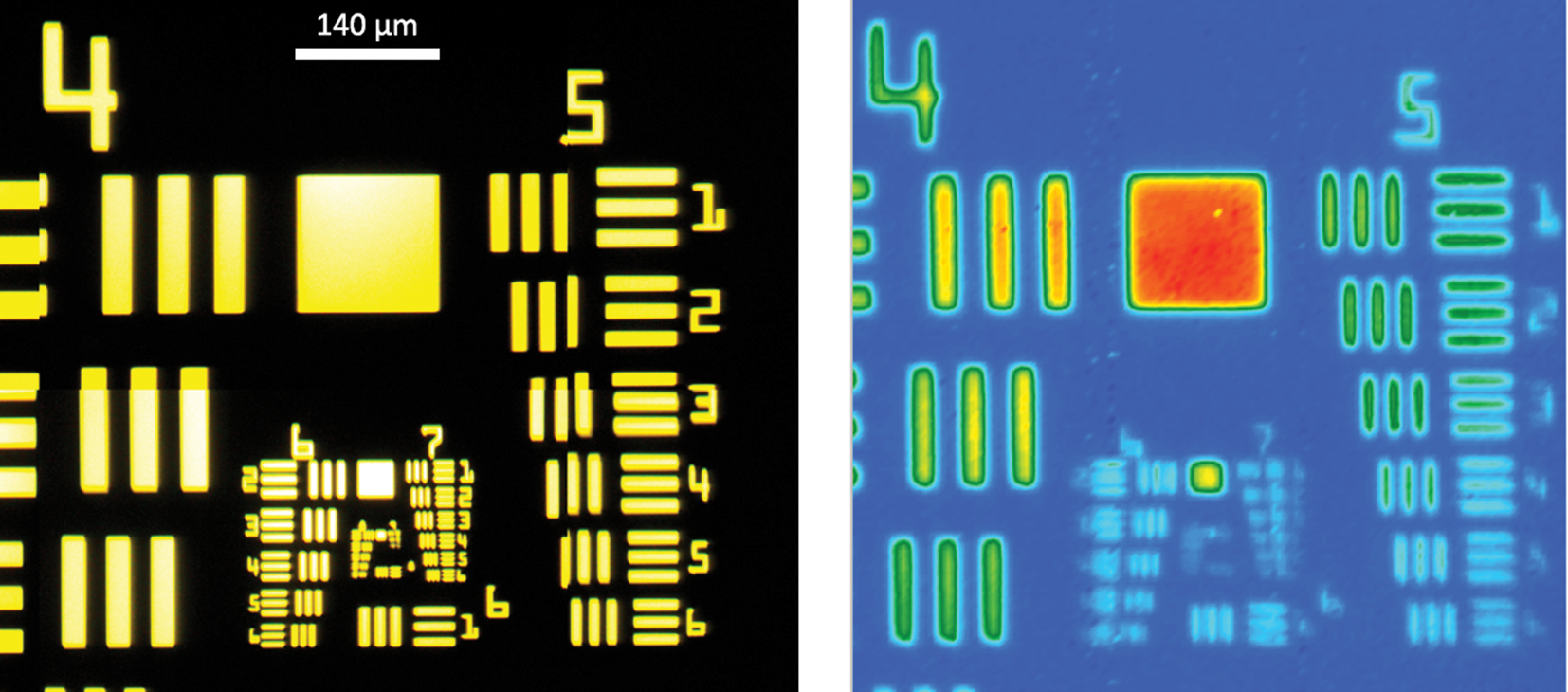
Figure 2: Images of a 1951 US Air Force standard-resolution target obtained with a visible camera (left) and infrared focal plane array camera (right). Each image size is 700 μm × 700 μm.
Figure 3 illustrates the wavelength dependence of spatial resolution for two objective numerical apertures used in commercially available FT-IR and direct quantum cascade laser (QCL) based systems. This contrasts with spatial resolution for the O-PTIR system, which has a theoretical spatial resolution of ~416 nm and is independent of IR wavelength. This is due to the spatial resolution of O-PTIR being defined by the wavelength of the probe laser (532 nm), whereas with FT-IR/QCL systems the spatial resolution is reduced by up to 30× and varies over the range of IR wavelengths.
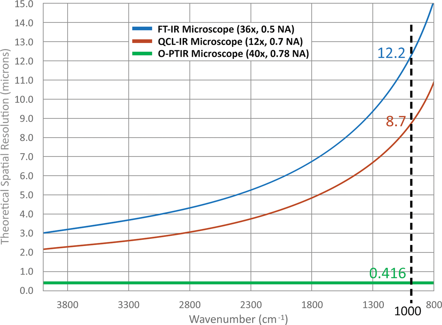
Figure 3: Theoretical spatial resolution comparison of FT-IR, QCL, and O-PTIR microscopes as a function of wavenumber. At 1000 cm−1, the theoretical spatial resolutions of the FT-IR, QCL IR, and O-PTIR microscopes are 12.2, 8.7, and 0.416 μm, respectively, assuming a 532 nm probe laser for the O-PTIR microscope.
Sample preparation prior to IR analysis can be complex and requires expertise. The best quality and the most accurate FT-IR data are collected in transmission mode. This requires a sample thin enough for the IR light to pass through without band saturation. This often requires sectioning of the sample to less than 20 μm in thickness, which can be time-consuming, difficult, or impossible.
Another common measurement mode in FT-IR is micro-attenuated total reflection (ATR), which minimizes the amount of sample preparation required and enhances spatial resolution through the use of high refractive index internal reflection element (IRE) materials, typically Ge, ZnSe, or diamond (Figure 4). With this method of analysis, the IRE of the ATR accessory or microscope objective must be in intimate contact with the sample. The sample stage is then adjusted to apply enough pressure to maximize the contact of the IRE with the sample surface. Applying too much pressure may cause damage to both the sample and/or the IRE, so care must be used. When comparing ATR and transmission spectra from a sample, there are spectral differences, including changes in peak intensities and peak positions.
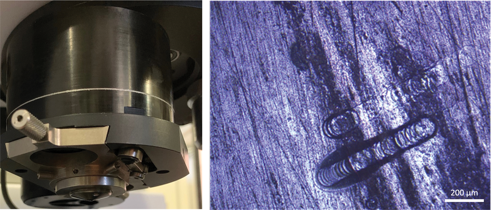
Figure 4: Example of an ATR microscope objective. Such measurements require sample contact, can affect native orientations, and are subject to cross-contamination, as shown on the right. Image size is 1.53 mm × 1.15 mm. μATR can be extremely useful, but pressure needed for intimate contact can damage the sample or μATR. It may cost several thousand dollars to repair a μATR.
Ideally, one would like to simply reflect an IR beam off the top surface of a sample to get a spectrum. Unfortunately, most samples reflect weakly in the mid-IR range and produce noisy spectra with dispersive artifacts. This makes comparison and ratioing of peaks problematic when compared to transmission data. Figure 5 illustrates how the IR spectrum of the same material measured in transmission can vary depending on the size of the particle being measured [Reference Bassan1].
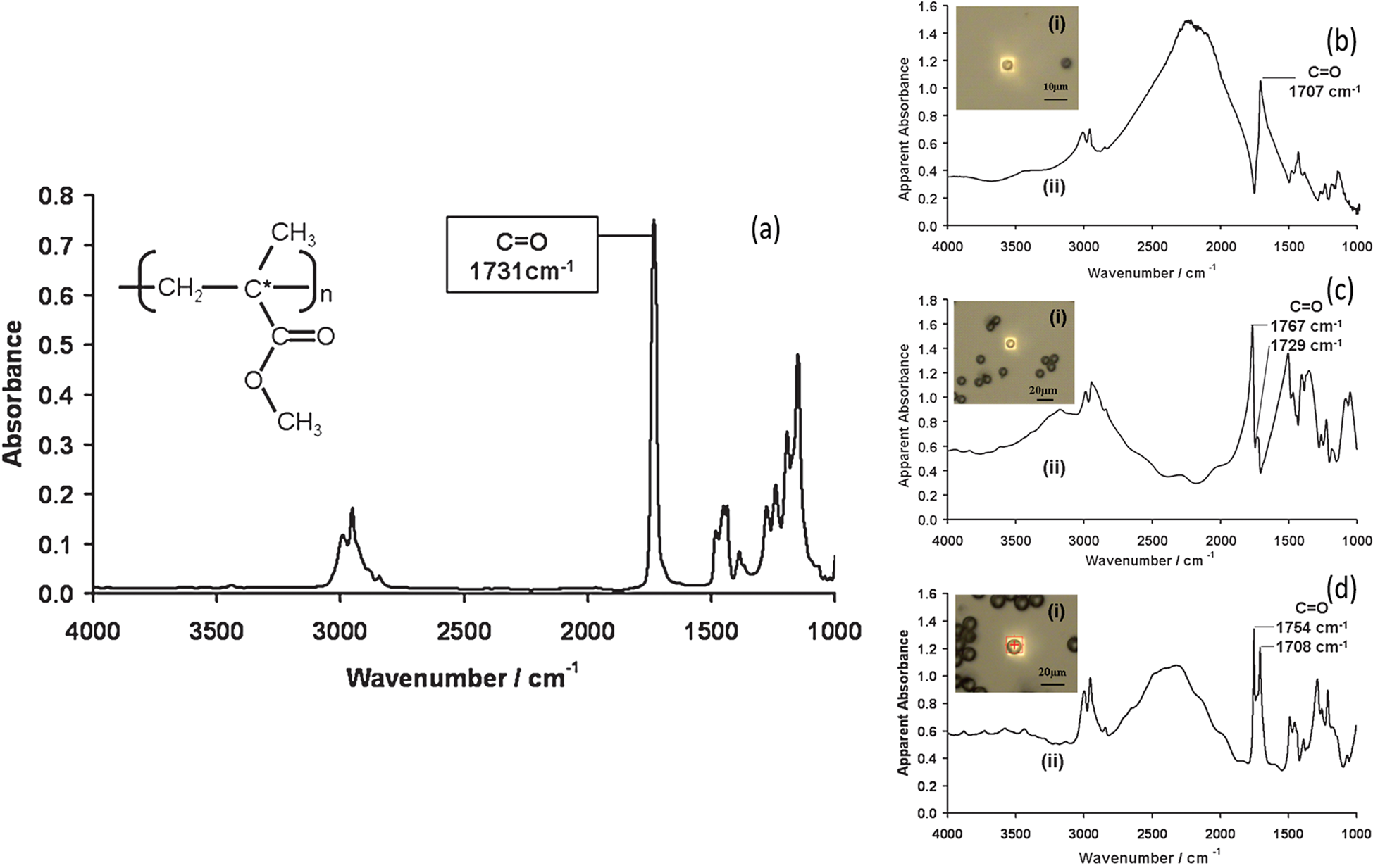
Figure 5: (a) The infrared transmission spectrum of a thin film of PMMA deposited on CaF2. The optical images (i) and the infrared transmission spectra (ii) of isolated (b) 5.5 μm, (c) 10.8 μm, (d) 15.7 μm diameter PMMA microspheres deposited on CaF2. Adapted from Figures 1 and 2 of [Reference Bassan1], with permission.
O-PTIR spectroscopy is a patented technology used exclusively in the commercial mIRage infrared microscope. O-PTIR overcomes all of the problems mentioned above that have hindered the expansion of FT-IR applications. The approach is based on a pump-probe architecture that couples broadly tunable pulsed IR laser sources (the pump) capable of covering the standard IR spectral range, with a short-wavelength visible laser (the probe) to provide submicron IR spectroscopy. In addition to achieving submicron IR spatial resolution, the mIRage system typically operates in reflection mode, does not require sample contact, and produces artifact-free IR spectra, such as those shown in Figure 6 for three common polymers. The unique architecture of this pump-probe system takes advantage of the fact that the probe laser (532 nm or 785 nm) can simultaneously act as a Raman excitation source, thus providing simultaneous IR and Raman spectroscopic analysis of the same sample location and at the same spatial resolution. Such a combination provides complementary IR and Raman spectral information that can help solve a chemical problem or provide a confirmatory analysis of an unknown contaminant.
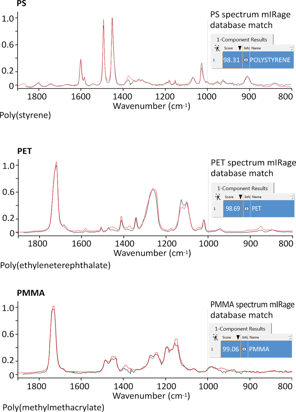
Figure 6: Comparison of the O-PTIR spectra of three polymers: poly(styrene) (PS); poly(ethyleneterephthalate) (PET); and poly(methylmethacrylate) (PMMA) with thin film-transmission spectra of these materials found in the KnowItAll™ IR spectral database (Wiley). The matches are excellent, even though the O-PTIR spectra were obtained in a reflection-like measurement on much thicker samples. If using FT-IR in transmission mode, it would be impossible to obtain unsaturated spectra from these samples because they would be optically too thick.
This ease of sample preparation allows the analysis of manufactured products like extruded or electrospun fibers to be measured without changing the mechanical properties induced by cutting, melting, or pressing into thin films, thus allowing the study of these materials in their native metrological forms.
Innovation
The O-PTIR technique provides infrared spectroscopy and chemical imaging with submicron spatial resolution that is up to 30× better than the conventional mid-IR diffraction limit, does not require contact, does not require thin sections to minimize saturation, and provides wavelength-independent spatial resolution. The O-PTIR technique has been developed by researchers at the Naval Research Laboratory [Reference Furstenberg2] and other groups [Reference Mërtiri3–Reference Li14] and has recently become commercially available [15]. There are multiple mIRage installations around the world at industrial companies, government research facilities, and major academic institutions for multiple reasons, including improved spatial resolution, and non-contact data acquisition that does not require the use of an atomic force microscope (AFM) and uses similar optical methods to FT-IR and Raman microscopy.
The O-PTIR technique has previously been used to study chemicals [Reference Furstenberg2], liquid crystals [Reference Mërtiri3], polymer particles and films [Reference Li5,Reference Zhang7–Reference Marcott9], biological tissues [Reference Mërtiri4], cells [Reference Zhang7,Reference Klementieva10,Reference Li12] and living organisms [Reference Zhang7], and pharmaceuticals [Reference Li14]. The O-PTIR technique provides an elegant non-contact way to chemically identify contaminants with higher spatial resolution than conventional IR microscopes, while maintaining the advantages of an optical microscope-based platform. O-PTIR has been referred to by several names and acronyms including photothermal IR imaging spectroscopy (PT-IRIS), mid-IR photothermal (MIP), mid-IR photothermal microscopy, and IR photothermal heterodyne imaging (IR-PHI). We prefer O-PTIR because it is both easy to pronounce and suggestive of optical IR, which in turn alludes to two of the key advantages: (1) better spatial resolution is achieved through a (visible) optical probe beam that can be focused much smaller than the IR beam; and (2) the technique is based on optical microscopy. O-PTIR builds on prior work in visible light photothermal imaging and spectroscopy [Reference Harada16–Reference Boyer19] and photothermal infrared standoff detection techniques [Reference Farahi20–Reference Papantonakis22].
A schematic diagram of the O-PTIR technique is illustrated in Figure 7. O-PTIR uses a visible probe beam to detect the photothermal response of IR-absorbing regions of a sample. The sample is first illuminated with an IR beam from a pulsed tunable IR laser source, for example, a QCL or an optical parametric oscillator (OPO) laser. When the IR source is tuned to a wavelength corresponding to an IR absorption band in the sample, a portion of the IR light is absorbed and converted to heat causing a temperature increase in the IR-absorbing regions. This temperature increase results in local heating and thermal expansion that causes changes in the refractive index. Refractive index changes are in turn detected by focusing a shorter-wavelength visible laser beam (for example, green at 532 nm) that overlaps the IR-illuminated region onto the sample surface. Changes in the reflected green light intensity are then monitored using a visible light detector. The spatial resolution achieved by O-PTIR (Equation 1) is set by the wavelength of the visible probe beam rather than the wavelength of the IR beam. The spatial resolution improvement is determined by the ratio of the IR wavelength to the probe wavelength.
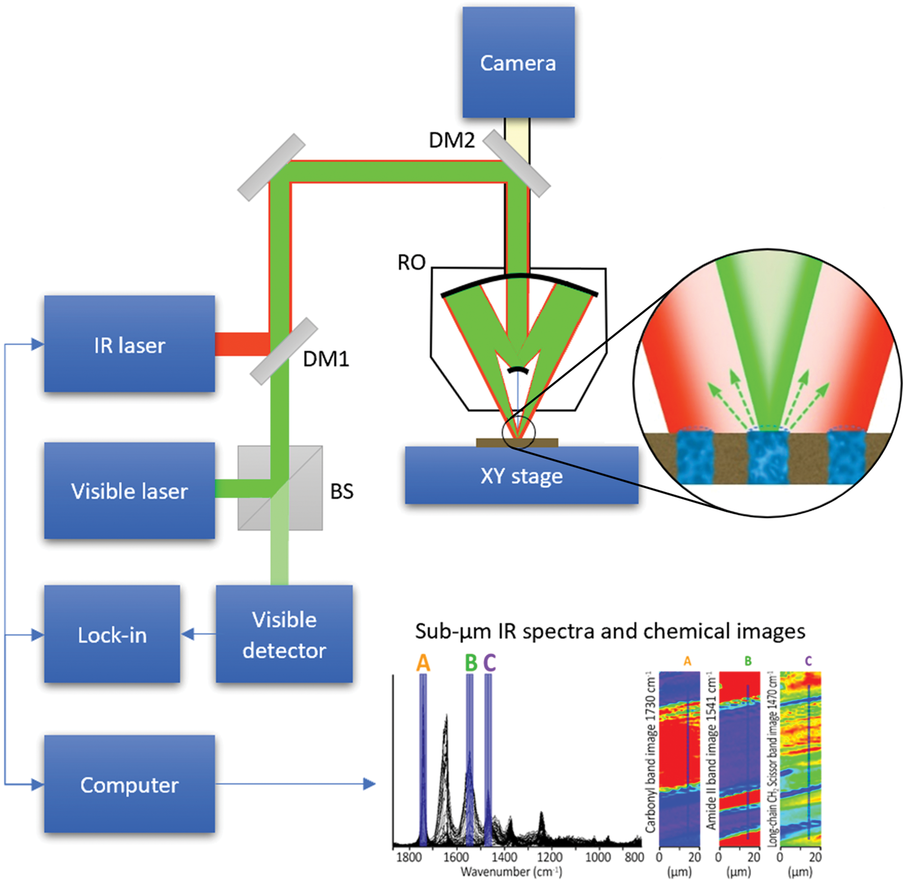
Figure 7: O-PTIR technique schematic diagram. Visible and pulsed IR laser beams are combined colinearly through a dichroic mirror (DM1) and focused on a sample via a reflective objective (RO) of a Schwarzschild design. When the IR laser is tuned to a wavelength corresponding to an absorbing band of the sample, the absorbed IR light causes local heating and thermal expansion in the IR-absorbing regions of the sample (zoomed inset). This IR-induced photothermal distortion causes a change in the intensity and/or angular distribution of visible light reflected/scattered from the sample. The visible light can be collected by the same reflective objective (or alternately in transmission, not shown). Reflected visible light passes through a beam splitter (BS) and is measured by a visible detector. The intensity of the detected visible light is synchronously demodulated with a lock-in amplifier at the frequency of the IR laser pulses. IR absorption spectra can be created by measuring the amplitude of demodulated visible light while sweeping the wavelength of the IR laser source. Chemical images can be created by measuring the IR absorption while scanning the sample on an XY stage under the IR and visible laser beams. Submicron spatial resolution can be achieved because the visible beam can be focused to a much smaller spot than the IR radiation. A second dichroic mirror (DM2) enables viewing of the sample via a conventional microscope camera and enables selection of regions of interest for IR measurements. Measurements in this article were performed on a mIRage infrared microscope using the O-PTIR technique.
Another key advantage of the O-PTIR approach is that the spectra produced do not contain scattering contributions, thus the intensities are directly proportional to the actual amount of light absorbed by the sample. As a result, the signal from an O-PTIR measurement produces a more “pure” absorbance spectrum, devoid of non-absorbance contributions like dispersive reflectivity responses. This means that O-PTIR spectral peak positions, line shapes, and relative intensities are more likely to match those obtained by transmission IR measurements. This is true even if these signals are collected in reflection mode (far-field), which has major practical and ease-of-use benefits.
Results
Collection of O-PTIR data.
The following examples show results from a small subset of samples that were characterized by Seagate Technology with the mIRage instrument. Multiple samples were loaded and spectra collected at over 60 locations. Figure 8 shows spectra from two contaminant locations. The top image (Sample A) shows a particle recessed near a feature of the device and the O-PTIR spectrum recorded at the location indicated by the arrow, while the bottom image (Sample B) shows a similar contaminant and its corresponding O-PTIR spectrum over a recessed edge. These samples could not be measured with traditional FT-IR methods since the ATR objective would have been obstructed before contact with the contamination occurred. The mIRage instrument can be fitted with different IR pulsed laser sources, allowing measurements over the standard IR spectral range (3600–800 cm−1). This broader spectral range can aid in the identification of materials that may have similar spectra in the fingerprint region (1800–800 cm−1). In this example, the O-PTIR spectra of both contaminant particles are consistent with a polyamide such as nylon, as indicated by comparison to the red nylon reference from the KnowItAll™ IR database (Wiley).
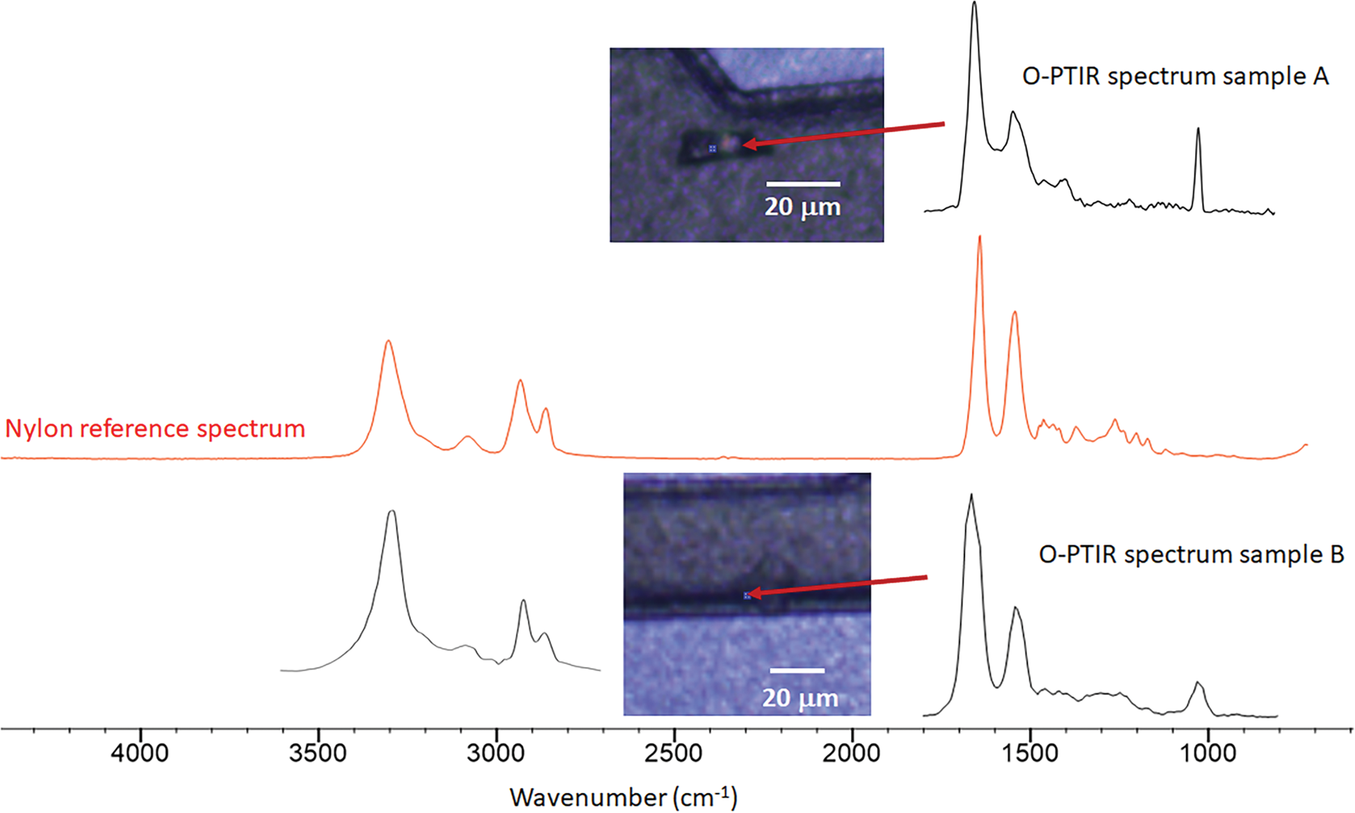
Figure 8: Optical images and O-PTIR spectra of sample A (top) and sample B (bottom) from two locations indicated by the red arrows where there were unidentified organic contaminants on the surface of a recording head. The middle red spectrum of nylon was obtained via a digital search of the KnowItAll IR database.
Figure 9 shows an example of the improved spatial resolution achievable with O-PTIR as compared to conventional diffraction-limited FT-IR measurements. The arrow indicates a particle (approximately 5 μm) that was identified via a library match of its O-PTIR spectrum to a KnowItAll™ IR library spectrum of polyetherimide.
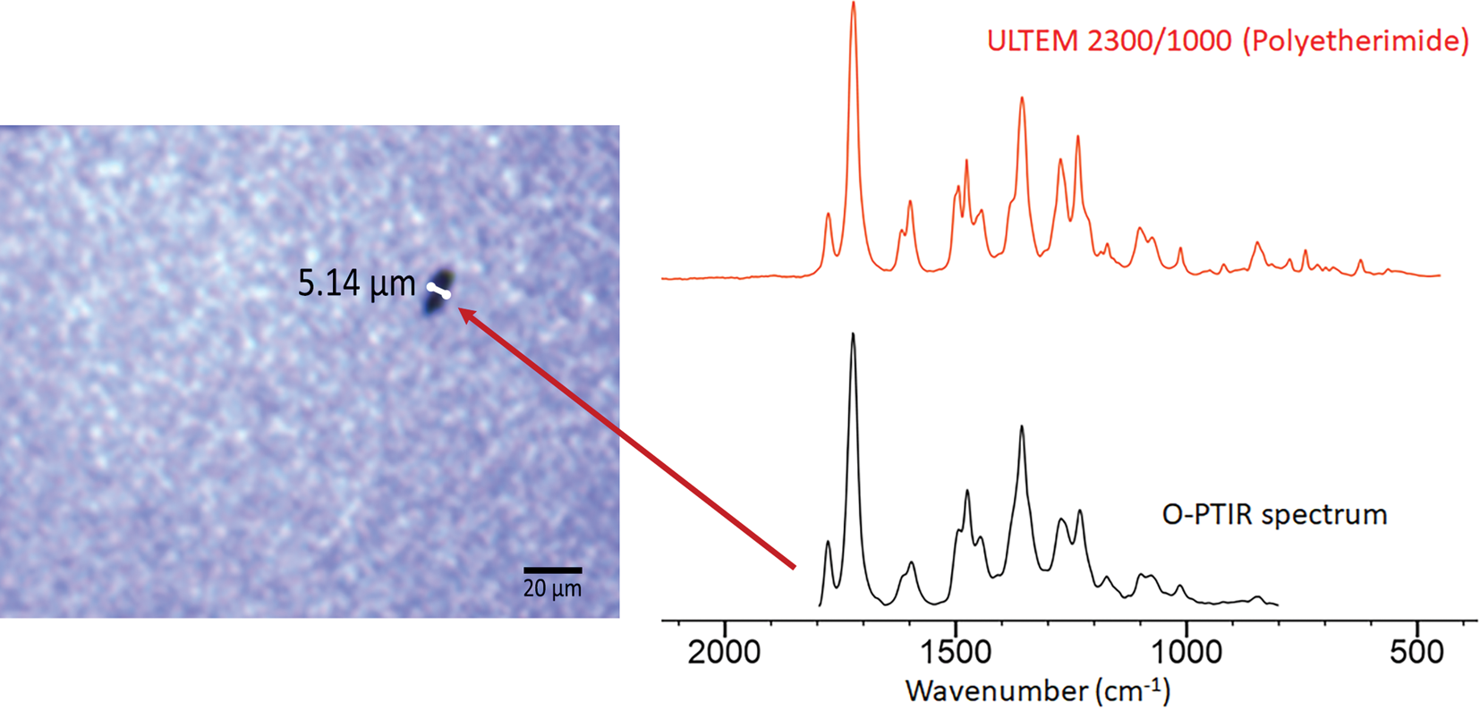
Figure 9: Optical image showing a ~5 μm defect on the surface of a recording head. The O-PTIR spectrum collected from the center of the defect is an excellent match with the reference spectrum of a polyetherimide found in the KnowItAll database of digitized IR spectra.
Collection of combined O-PTIR and Raman microscopy data.
The complementarity of IR and Raman is well known and is often why analytical laboratories have separate IR and Raman microscopes. However, to take full advantage of the complementarity the challenge is that for samples or regions of interest that are only a few microns in size, moving from an IR to Raman microscopes, or vice-versa, presents sample location and registration difficulties. An additional advantage of simultaneous IR + Raman is that it is also confirmatory. Unknown IR spectra can be searched against databases, and to confirm this search, simultaneously collected Raman spectra can be searched against Raman databases, or vice versa. As such, submicron IR + Raman data provide both complementary and confirmatory capabilities for identification of unknown materials, with better accuracy and confidence.
A new capability recently added to the mIRage system is simultaneous collection of O-PTIR and Raman spectra of the same sample location with the same submicrometer spatial resolution (Figure 10) [Reference Marcott9,Reference Li23]. This is possible by use of a Raman-grade laser to measure the O-PTIR response. In the IR + Raman configuration, the Raman-shifted light is simultaneously diverted to a spectrograph, thus providing simultaneous, same spot, same spatial resolution O-PTIR and Raman spectra. This new capability aids in the identification of organic and inorganic materials using both techniques. Raman is also used to examine coatings, stress/strain relationships, and various applications in electronics and other industrial fields.
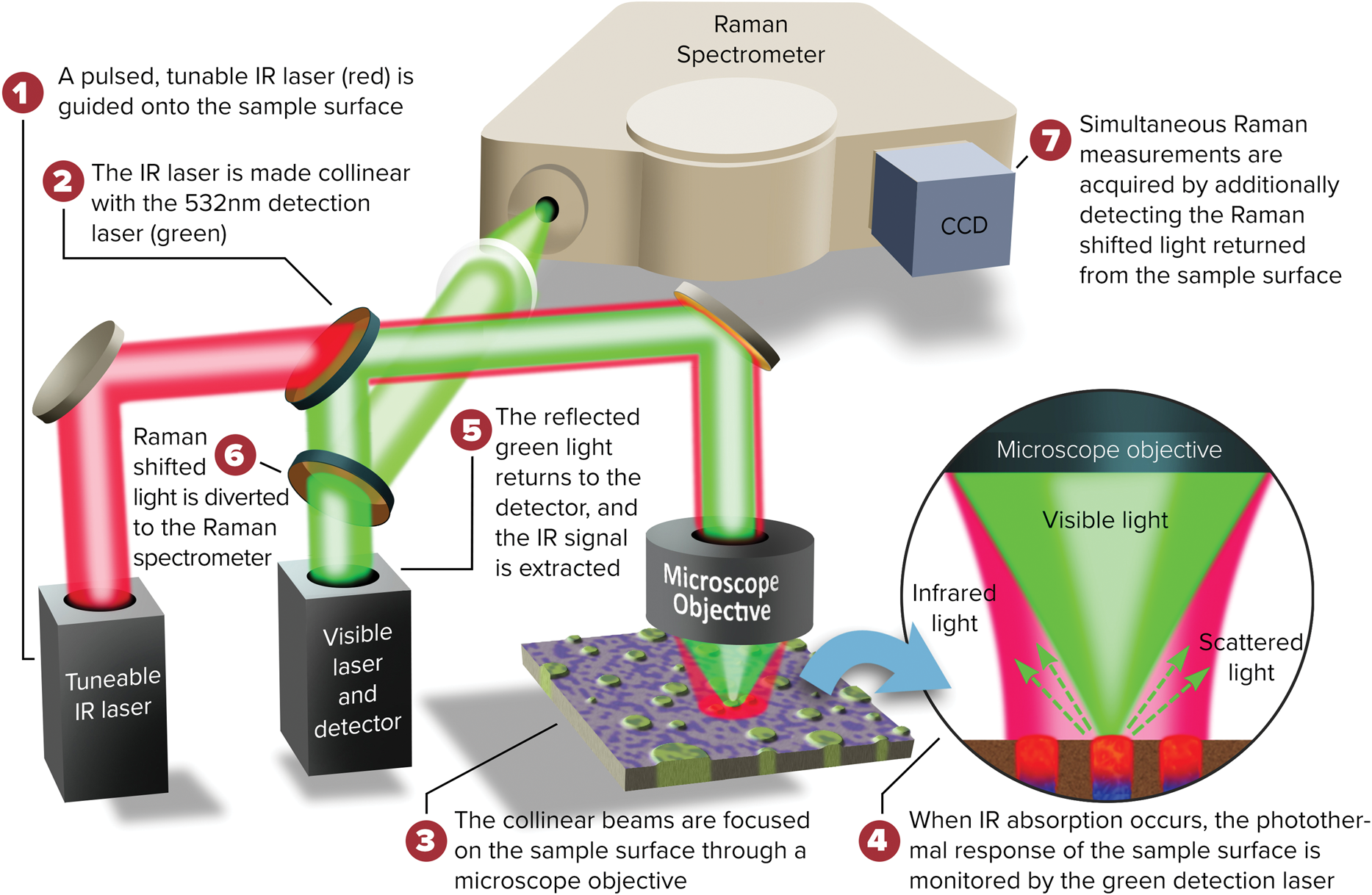
Figure 10: Diagram of the combined O-PTIR plus Raman instrumental setup.
Figure 11 shows an example of the complementary and confirmatory O-PTIR and Raman spectral information that can be collected in reflection mode from a contamination particle that is ~10 μm long and 2 μm wide. The O-PTIR and Raman spectra were simultaneously collected from the same spot and at the same spatial resolution. Although collected in reflection mode, the O-PTIR spectrum is comparable with data taken from pure samples in transmission mode. When the spectra were digitally searched against KnowItAll IR and Raman databases, it was determined that this particular contaminant is likely a polyether material.
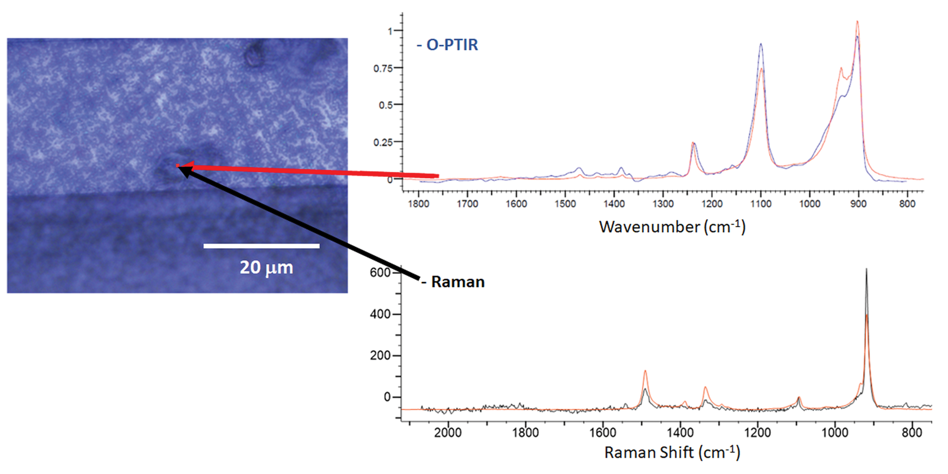
Figure 11: Optical image showing a defect on the surface of a recording head. Simultaneously collected O-PTIR and Raman spectra collected from the defect site were searched using KnowItAll against their commercial digital libraries. The best matches in each case (shown in red) were polyether materials.
The contaminates identified in these measurements include a small subset of the measurements Seagate has measured using mIRage. The contamination includes a variety of materials plus foreign particles that can be introduced during research and development and include polymers, lubricants, etc. For this evaluation the mIRage was able to achieve better than 90% chemical identification.
Additional Examples of O-PTIR Applications
In February 2019 the Taiwan Semiconductor Manufacturing Company (TMSC) used a photoresist that included an abnormally treated element that created a foreign polymer in the photoresist resulting in an estimated loss of $550 million [24]. Systems that better identify contaminants quickly with minimal sample preparation and higher spatial resolutions while using typical training for optical microscope systems is needed to minimize these losses. Defect analysis is a major application area for O-PTIR spectroscopy. Failure analysis using conventional IR microspectroscopy has been significantly hampered by lack of spatial resolution, poor sample contact with the IRE in ATR measurements, and uninterpretable spectra in direct IR reflection mode.
Figure 12 shows an ultrasonic welding application used to make electrical connections for electronic devices. Raman microspectroscopy could have provided the spatial resolution required for such an analysis, but the dark color and strong fluorescence prevented effective chemical analysis of the weld defect with Raman microscopy. O-PTIR spectroscopy provides high spatial resolution even when the sample fluoresces. The O-PTIR spectral features in the defective zone suggest there was an excess of flux, which is typically used to prevent the oxidation of the solder. In this case, the contamination effectively prevented the solder from wetting the pad and forming a proper weld. Single wavenumber O-PTIR images collected at 1724 cm−1, where a properly formed weld would have a strong spectral feature, shows the extent of contamination in the defective device.
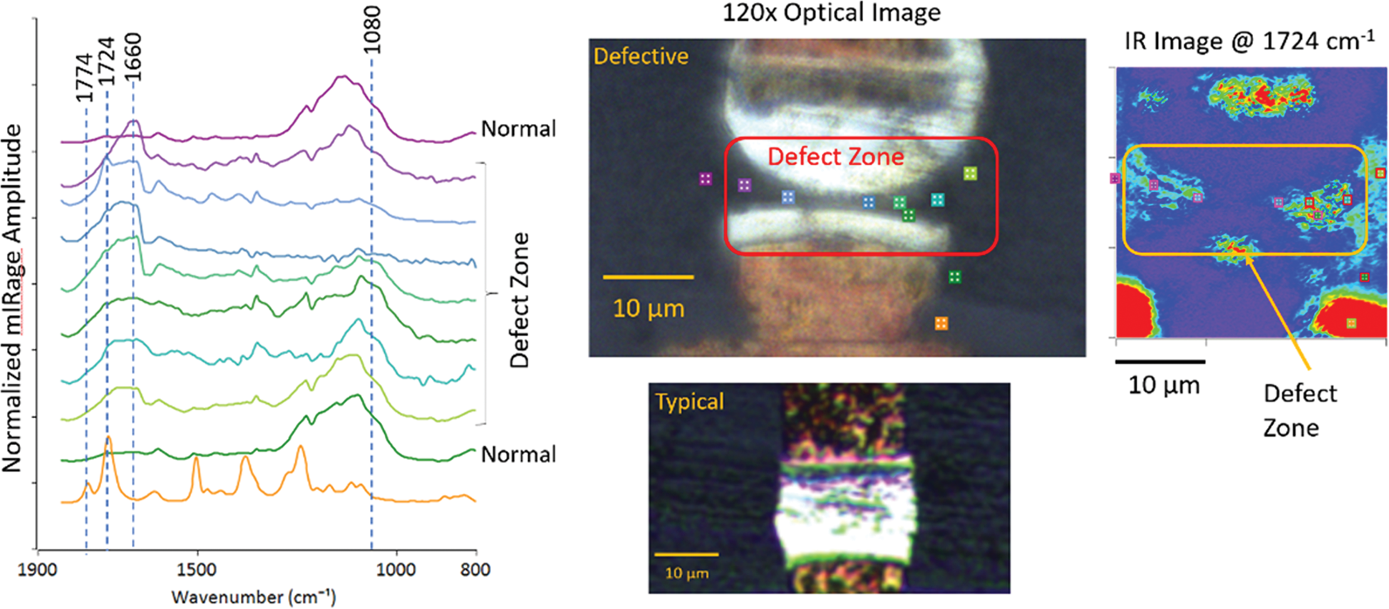
Figure 12: Optical images show a good weld and a defective weld in an electronic component. O-PTIR spectra were collected at the color-coded locations in the image in and around the weld defect (left). The IR absorbance image on the right was collected with the QCL tuned to 1724 cm−1, where a properly formed weld has a strong absorption band. Red indicates regions of strongest absorbance at 1724 cm−1.
There are many cases where contamination is not directly accessible with conventional IR instrumentation. Figure 13 shows a 20 μm dark contamination that is underneath the thin metal film, as can be seen from the white circular delamination of the metal film due to the protrusion from this defective thin-film transistor display. Use of conventional ATR microscopy would have been limited by presence of the thin film, obstructing direct access to the contamination particle. The sample was able to be analyzed via O-PTIR without additional sample preparation or the need to perform any physical extraction of the particle. Both the pump IR and probe-visible lasers penetrated the thin metal film and were focused on the contamination that lies beneath. The probe laser detected the photothermal expansion of the particles and was reflected back through the metal film and onto the photodetector. Examination of the spectra, particularly the presence of the strong broad IR absorbance band at the 1706 cm−1 band, suggests that this suspect contamination particle may have been a vulcanized styrene-butadiene rubber (SBR) that has oxidized to form a carboxylic acid.
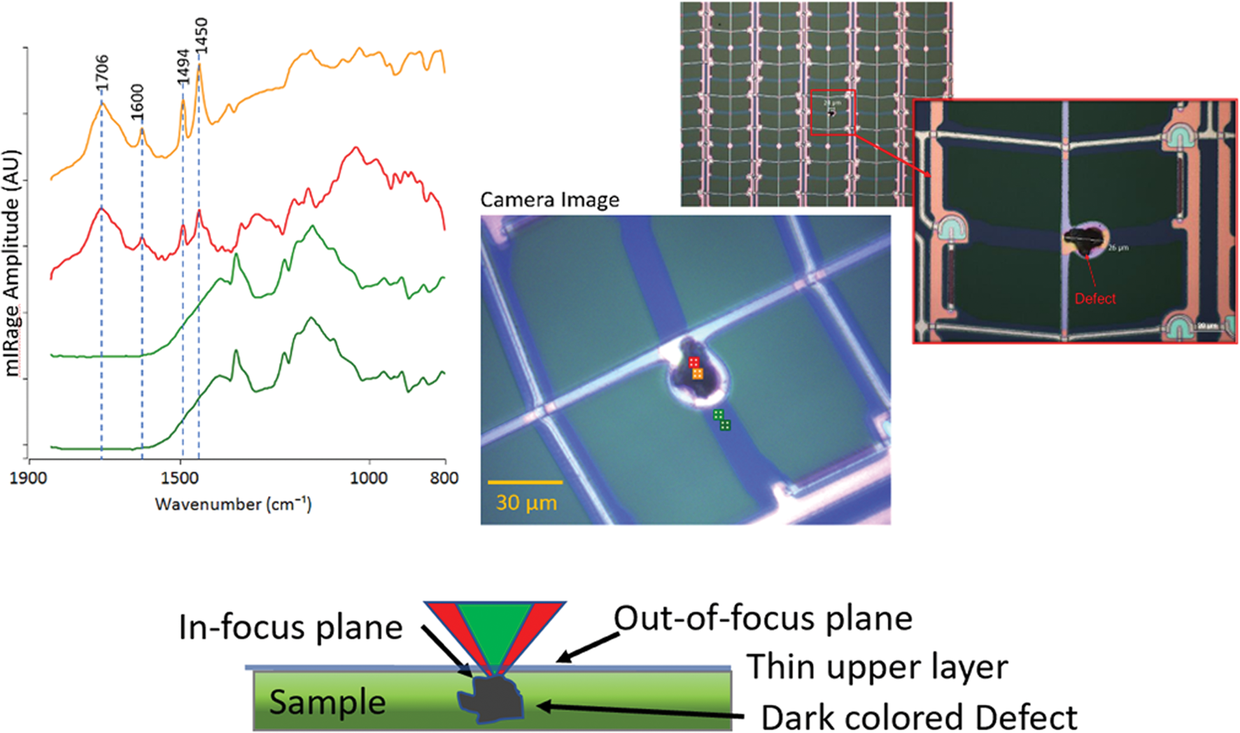
Figure 13: O-PTIR analysis of a dark contaminate particle in a thin-film transistor display. In-focus confocal-like IR measurements can be performed through the thin partially transmitting metallic overlayer enabling spectral identification of the contaminant. The red and orange spectra collected from the locations shown on the image are from the location of the contaminant.
Conclusion
We have introduced a new IR microscopy modality called O-PTIR spectroscopy that can be coupled to Raman microscopy for submicron simultaneous IR and Raman microspectroscopy. Seagate chose the mIRage system to improve characterization of contamination earlier in the research and development of new manufacturing processes. The fundamental principles and examples presented here display the advantages of O-PTIR in the identification of defects and contamination in hard drive and related electronic industries. O-PTIR spectroscopy has the potential to be disruptive in the important and growing field of IR microspectroscopy. Key advantages of O-PTIR over the technologically mature and traditional FT-IR microspectroscopy approaches include submicron IR resolution; collection of spectra in far-field (non-contact) reflection mode that are FT-IR transmission-like, yet free of scattering artifacts; confocal-like measurement; and simultaneous Raman analyses. mIRage is a unique and vastly more useful measurement capability. Application areas are increasing and encompass all the traditional FT-IR fields such as polymers, defect analysis, and life science. Further adoption by the IR and Raman community will fuel exploration into new ways O-PTIR will break new limits.


