


Introduction
Scanning electron microscopy (SEM) has long been a mainstay scientific instrument for the study of morphology and composition on the micro- and nano-scale. Energy-dispersive X-ray spectrometry (EDS) systems provided the means to determine the phases present (via inference from elemental X-ray analysis) in materials examined in the SEM.
Each advance in EDS technology has supported a concurrent expansion of the information available to the materials analyst. The advent of silicon drift detector (SDD) systems and spectral imaging data storage facilitated EDS acquisitions to produce element maps and other data [Reference Thompson1]. The spectrum image stores an entire spectrum at each pixel in the image, and various types of software are used to extract useful information from this data cube. The addition of a motorized stage enabled multiple scan rasters to extend small-scale analysis over relatively large areas of the material (length scales of several millimeters). The next logical step involved automated techniques that use electron image capture followed by EDS analysis in regions of significance selected from the contrast within the grayscale electron image. In this way, large-area electron imaging followed by EDS chemical typing gave rise to automated quality control and materials inspection tools. The most prominent example may be in mining applications [Reference Gu2, Reference Pirrie3].
This article reviews the concept of large-area quantitative phase mapping using a multivariate statistical approach known as principal component analysis (PCA) [Reference Kotula4–Reference Shlens6]. In this case the term “large area” refers to an analysis area on the order of 1 mm2 or greater. Phase mapping has the advantage of greatly reduced analytical ambiguity because the phase identifications are developed by a user-independent algorithm residing within the “engine” of the EDS system. Typically, the number of phases will not exceed a maximum of 15 to 20 within a material, and more normally the number is in the 5 to 8 range. Even when the results contain up to 20 phases, each with a well-defined chemistry, the data are presented in a compact enough form for direct interpretation. A set of X-ray element maps via EDS, by contrast, may contain up to 20 elements spread over a million pixels and across many phases. This presents a more daunting analytical interpretation: which elements are bound to which other elements in which phases.
The concept of large-area phase mapping is not new [Reference van Hoek7–Reference Ruffell9]. However, previous techniques employed to create phase maps render large-area phase mapping impractical. Traditional element-based phase mapping requires at least an order of magnitude increase in the number of X-rays per pixel as compared to straightforward EDS element mapping, where roughly 5,000 X-rays per pixel—the sum of all X-rays collected in the spectral imaging data set divided by the total number of pixels—are needed for a robust element map. Additionally, every element, including those at trace levels, should be properly identified for the validity of this technique to be optimized. Similarly whole spectrum-based phase mapping [Reference Nylese and Anderhalt.10] has the same limiting requirements because several thousand X-rays per pixel are required to properly compare spectra from adjoining pixels with statistical certainty.
Fortunately, the principal component-analysis technique described in this article requires far fewer X-rays per pixel than that required for basic EDS X-ray element mapping. It is well-established that PCA requires only 25 to 150 X-ray counts per pixel to yield good results, and the implementation described here involves—actually requires—no user interaction. As with most spectrum imaging systems, it also has the additional advantage of requiring no prior knowledge of the elements present.
Materials and Methods
Samples for analysis
All samples for analysis were mounted in a bakelite mount, polished with successively finer grit paper, followed by polishing with 9 µm, 3 µm, and then 1 µm diamond slurries. The samples were coated with 100 nm of carbon to prevent charging. The first sample was a crushed rock from a mine. The rock was pulverized and sieved through a mesh with 250 µm openings. The goal of this analysis was to determine the quantity and distribution of the specific minerals within the rock and the locked and liberated fraction of each mineral after pulverizing. The second sample was a polished section of a complex ceramic composite. The end-user application required determination of the size, areal fraction, and distribution of the phases present.
Instrumentation
The results presented here were obtained on a JEOL JSM-7001F field emission SEM. The electron microscope was operated at a 15 kV accelerating voltage and 12 nA probe current. The EDS data were collected with a pair of 30 mm2 Thermo ScientificTM UltraDry EDS detectors mounted at a 35-degree take-off angle and 55 mm from the sample. These detectors were mounted 120 degrees relative to each other. The geometry was based on available high-angle ports. Collected X-ray events were channeled from each X-ray detector into independent pulse processors that discriminated legitimate X-ray events from background and determined the energy of each X-ray event. These digitized energy events were then collected by a “headless” computer along with their position coordinates from the electron beam scan controller to create a spectral imaging (SI) data set. This SI data set was then transferred to the computer that operates the Thermo Scientific Pathfinder software with which the user performs EDS X-ray acquisition and data analysis.
Principal component analysis
The critical technology that enables large-area, quantitative phase mapping is principal component analysis (PCA). The commercial implementation of PCA as provided by Thermo Fisher Scientific is called COMPASSTM. Principal component analysis is predicated on the assertion that a small number of dominant components can very nearly, although not perfectly, describe an arbitrarily complex system. An example of this is the classic red-green-blue color set that creates the full range of colors displayed in a digital image or video. While one may perceive thousands or millions of colors in an image, every pixel in that image is actually some combination of the original three-color components. The technical background to PCA is described in detail elsewhere as a general technique [Reference Shlens6], and it applies to EDS spectral imaging analysis [Reference Kotula4, Reference West5].
There are several benefits to this technique as applied to EDS phase mapping. The first is that very complex data sets can be described by a relatively small number of dominant components (that is, 3 to 20) that are more easily handled for interpretation. Moreover, because it is customary to identify each component, this method is effective at locating minority phases or phases that are differentiated only by the presence of a trace element. The statistical nature of the algorithm prohibits user intervention, rendering the technique free of human bias. The final and possibly most important advantage to large-area phase mapping is that the dominant components can be extracted even when there are relatively few X-ray counts in the individual spectrum for each pixel. As a result, the dominant component maps are extracted with somewhere between 25 to 150 spectrum X-rays per pixel. Because the required X-ray collection is now reduced by a factor of roughly 50–100 times as compared to element mapping, the data acquisition process is shortened significantly.
For the technique described here, these principal component maps must be translated into phase maps. In a PCA map, every pixel has a finite statistical probability of belonging to any given component. In a phase map, each pixel belongs to just one—and only one—phase. This enables both quantitative analysis of the EDS X-ray spectrum within each phase and the quantitative measurement of the size and distribution of each phase. Translating the component maps into phase maps is accomplished using the same types of intensity thresholding algorithms used for traditional element-based phase mapping. The spectrum for each phase is the sum total of the spectra from each pixel in the phase. The identity of each phase is then determined either by quantitative analysis of the spectrum or by matching against an X-ray spectral library. At the end of this process, the identity of each phase was closely identified, given that uncertainties can arise from strong fluorescence effects, spatial sampling frequency, and the possible presence of polymorphs, for example, rutile versus anatase for TiO2.
Results
Analysis of crushed mining sample
Number of distinct phases.
Figure 1 shows a low-magnification backscattered electron (BSE) image of some grains in a crushed rock sample from a mining operation. Figure 2a shows the grayscale SEM image, exhibiting atomic-number contrast from backscatter electrons, of a single grain similar to that selected in the red box of Figure 1. If the operator had no other clues to the locations of the various phases, the EDS system could be used to probe the light and dark regions to provide qualitative and quantitative analyses of what appear to be different phases. However, this procedure has limitations. One limitation is that the BSE image does not conclusively determine the number of phases present. Figure 2b shows an image histogram (number of pixels of each gray level) with thresholds set at what appear to be four intensity levels above the lowest few gray levels (which correlate with the carbon-based mounting material). Each threshold is marked by a color, and these colors are mapped to colorize the BSE image (Figure 2c). The enlarged-area color map (Figure 2d) shows four regions for EDS analysis. Performing an EDS analysis inside each of the identified regions could provide a qualitative and quantitative elemental analysis for each expected phase.

Figure 1 BSE image at 15 kV of crushed rock “grains” mounted in bakelite showing several mineral phases. Total field width is 1.03 mm. Red box shows a single “grain” similar to that analyzed in later figures.

Figure 2 Detailed analysis of a single grain extracted from a boxed region like that shown in Figure 1. (a) SEM image with brighter regions indicating higher atomic number in grayscale. Image width = 76 µm. (b) Threshold designations on the image histogram of (a) showing the numbers of pixels at each gray level. The four increasing brightness levels show four distinct phases: 1 (red), 2 (yellow), 3 (blue), and 4 (violet). (c) Color map of BSE intensities formed by thresholding the gray levels in (b). (d) Higher magnification showing the four “phases” selected for EDS analysis.
Element mapping.
It is still not clear that all of the phases have been found. Figure 3 shows X-ray maps for each element detected in this grain. Regions of major differences in material composition are identifiable by visual inspection. Neglecting the carbon from the mounting material, these element maps indicate the presence of at least six phases. Moreover, when three element maps are converted to red, green, and blue primary colors and combined, element associations can be easily discerned—but only three elements at a time. These qualitative X-ray maps tell us what elements are present and some element associations, but any composition more complex than just the major elements is difficult to determine. Quantitative analysis of a phase may be used to indicate its composition, but a phase is usually defined by its crystal structure. Moreover, solid solution effects can change the composition within certain crystal structures. Normally we would use a diffraction method, powder X-ray diffraction, or electron diffraction in the transmission electron microscope to determine the crystal structure by matching d-values to standard phases stored in a database (for example, the powder diffraction file databases of the International Centre for Diffraction Data).

Principal component analysis.
There is a quicker way to determine the identity of the phases present. By invoking multivariate statistical analysis and performing a principal component analysis, as described above, distinctive groupings of elements can be identified. Figure 4 shows COMPASS phase maps of the same grain examined in Figures 2 and 3. The Compass phase map for this sample was constructed with only 76 X-rays per pixel and required an acquisition time of 30 seconds. In this case seven distinct phases (beyond carbon-based mounting compound) have been identified as shown in Table 1.

Figure 4 COMPASS phase maps of the grain shown in Figure 2. COMPASS software reveals seven groups of associated elements in the spectrum image data cube that are likely to be actual mineral phases. COMPASS analysis of the data cube took between 1 and 6 seconds depending on the speed of the Windows PC. Image width = 115 µm.
Table 1 Phases found with COMPASS in one 33 µm scan width and the average atomic number of each. Seven mineral phases were found.

Why is the BSE image inadequate?
The additional phase regions not identified in Figures 2 and 3 all had similar electron-image contrasts to nearby phases. Because backscattered image contrast is directly related to the average atomic number of any given region, these missed identifications are not surprising when the average atomic number of each phase is calculated (Table 1). The following instances of similar average atomic number are worth noting because these pairs are difficult to discriminate in BSE images:
-
∙ Sphalerite (ZnFe)S and chalcopyrite CuFeS2 with average atomic numbers of 21.8 and 22.0.
-
∙ Titanate (CaO TiO2 SiO2) and pyroxene (CaO FeO2 SiO2), where only the Ti and Fe component are interchanged, have average atomic numbers of 12.0 and 13.1, respectively.
-
∙ Pyroxene ((FeMg)O2 SiO2) and K-feldspar (KAlSi3O8), where the average atomic numbers are 10.8 vs. 10.6.
Phase identification by spectrum analysis.
After selecting the distinct regions for analysis, sufficient X-ray counts must be present in the spectrum to properly type the selected region as a particular phase. Again, this is difficult for regions of similar composition and for regions where the presence or absence of an individual minority element may define a distinct phase. In order to gauge the X-rays required for reasonable elemental typing of phases within a region, three spectra from the chalcopyrite CuFeS2 region are displayed in Figure 5. The only difference in these spectra is the number of X-rays present. Figure 5 shows that the spectra from a single pixel, a selected region within the phase, and the entire chalcopyrite phase contain 162, 5,000, and 2,000,000 X-rays, respectively. The 162 X-ray spectrum is insufficient even for basic elemental identification because the Fe K-series peaks contain only a few counts, which could be spurious noise events, and because the Fe-L peak was misidentified as oxygen. The 5,000 X-ray spectrum is sufficient for basic elemental identification but not sufficient for quantitative analysis. The 2,000,000 X-ray spectrum is sufficient for both elemental identification and rigorous quantitative analysis to determine the phase type.

Figure 5 Spectra from the chalcopyrite CuFeS2 region of Figure 4. (a) A single pixel with 162 X-ray pulses. (b) An area with about 5,000 X-rays. (c) The entire CuFeS2 phase with 2 million X-rays.
X-ray counts required for phase typing.
It is noteworthy that COMPASS phase mapping was able to determine phase identities with so few counts in each pixel (76 counts per pixel). This is particularly true when comparing it with traditional EDS X-ray element-based phase mapping, which requires quantitative analysis of elements in a spectrum image data cube containing several thousand X-rays per pixel. The sparse spectrum in Figure 5a is clearly insufficient for element-based phase mapping. This limitation is demonstrated by generating element-based phase maps from this data set (Figure 6). These element-based phase maps are generated by defining one or more X-ray intensity thresholds for each of the element maps. This thresholding technique is similar to that used in Figure 2 to identify regions of interest within the BSE image. The combined thresholds from each element map are then used to determine areas of distinct elemental composition, that is, phases. The phases are then typed by either inspecting the major elements present or by matching against a spectral library. In this example, careful manual thresholding of each of the element maps results in the identification of the five mineral phases implied from earlier visual observation of the X-ray element maps. This falls short of the seven phases that were identified by COMPASS (Figure 4). For example, in this case, the pyrite (FeS2) and chalcopyrite CuFeS2 were not differentiated. However, the sphalerite (ZnFe)S was identified as distinct from the pyrite (FeS2). The threshold for Zn was sufficient to achieve differentation between chalcopyrite and sphalerite whereas the threshold for Cu was insufficient to differentiate between pyrite and chalcopyrite. With enough effort, it may be possible to extract all 7 phases. However, the human interaction (and bias), the manual effort, and the uncertainty involved create limitations for this technique.

Figure 6 Element-based phase map from the region analyzed in Figure 3 indicating the presence of five mineral phases. Image width=115 µm.
Large-area phase mapping.
Precision stage movements allow separate SEM image frames to be stitched together forming large-area images and maps. This is how a large-area COMPASS phase map can be constructed (Figure 7). Unlike the qualitative element maps shown in Figure 3, the COMPASS large-area phase map can be fully quantified. Each of the phases in Figure 7 may be put through the same sizing analysis typically performed on metallographic images. Information such as average area of each phase, % phase area, and average phase perimeter are easily extracted. Table 2 shows these results for the phase map in Figure 7. Note that over the entire field additional phases were found (14 in all). If desired, additional information such as parent-child phase composition of a particular grain and locked and liberated percentages may be extracted.

Table 2 Quantitative results from the COMPASS phase map of Figure 7 showing size characteristics for the 14 distinct mineral phases found.

Analysis of a ceramic composite
There are applications where image analysis plus EDS phase typing is not even practical. In this next example, large-area COMPASS phase mapping was applied to the analysis of a complex ceramic composite. Figure 8 shows the area analyzed was just under 1 mm2, at 4,096 pixels on each side with a square pixel size of 0.24 µm. Data were collected until an average of 120 X-ray counts per pixel was attained. The collection rate was 200,000 stored X-ray counts per second. Total collection time was approximately 3 hours.
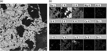
Figure 8 Large-area X-ray maps of an engineered ceramic composite (a) BSE image. Image width = 0.98 mm. (b) X-ray element maps from the area imaged in (a).
Figure 8a shows the BSE image for this ceramic composite. As in the previous example, however, the X-ray element maps (Figure 8b) provide only qualitative information about the large area analyzed. The COMPASS phase map in Figure 9, with the phases identified and classified by their majority components in Table 3, provides a better quantitative phase analysis of this engineered ceramic composite. The relative areal coverage of each identified phase is included in Table 3. Carbon accounts for approximately 40% of the analyzed area of the composite. The quantitative results indicate that the 11 non-carbon phases of the composite are metals, metal-oxides, sulfides, or sulfates. The elemental EDS maps (Figure 8b) qualitatively support this observation. While the phase map has been instructive and aesthetically pleasing, the results in Table 3 provide the detailed quantitative results upon which engineering decisions can be made. In this way, tabular results may be more valuable than the overlaid color phase maps themselves.

Figure 9 Large-area COMPASS phase map of ceramic composite. Image width= 0.98 mm. See phase legend in Table 3.
Table 3 Phase analysis of a ceramic composite shown in Figures. 8 and 9 showing the 11 mineral phases color coded to Figure 9.

Discussion
The phase analyses here by COMPASS software demonstrate the capability of identifying and quantifying phases of interest within a material with no user bias and no apriori knowledge of the material. Other techniques are either prone to incomplete results, such as EDS element-based phase typing of regions selected after image contrast thresholding, or require X-ray acquisition times that are not practical, such as element-based or spectrum-based phase mapping techniques. While electron imaging plus spot-mode analysis may not be as accurate as COMPASS phase mapping, a logical question is whether the former technique holds a speed advantage.
In the crushed rock sample analyzed in Figures 1 through 7, the EDS data was collected in single frames of 512x384 pixels for a frame time of 30 seconds. At 500,000 X-ray counts stored per second, this resulted in an average of 76 X-rays per pixel. This was sufficient to create the COMPASS phase map displayed in Figure 7 with a 2 µm pixel size. The complete large area phase map was analyzed in 30 seconds × 9 frames = 270 seconds.
The productivity of COMPASS phase mapping can now be contrasted with the productivity of using the electron-image contrast to identify the grains of interest followed by EDS spot-mode analysis within each grain for phase typing as shown in Figure 2. For the latter technique, the image acquisition of a single frame of sufficient imaging resolution would take between 2 to 5 seconds. This collection time depends on the efficiency of the BSE detector and the acquisition parameters of the electron microscope. The subsequent spot-mode analysis—assuming the need for 5,000 X-rays per spectrum for basic elemental typing of the grain and the defined collection rate of 500,000 X-rays per second—is roughly 10 milliseconds per grain times the number of phases in that grain (this method detected only 4 mineral phases in Figure 2). For the 2,233 grains identified in Figure 7 at 10 milliseconds per grain, it will take at least 22 seconds to type each phase. Some additional overhead to move the beam between pixels would be required, indicating an estimated total time to identify and phase-type the grains within this large area would be 89 seconds. Thus, electron image + spot mode EDS typing may be expected to run approximately 3 times faster than large-area COMPASS phase mapping. However, this basic typing provides no quantitative analysis of each grain, thereby leaving open the opportunity for serious omission of phases and misclassification of phases in many of the grains. COMPASS phase mapping, while taking somewhat longer, provides a more accurate and reliable means of phase detection and determination. The two techniques provide a different approach and a trade-off between information speed (that is, how fast one can collect the data) and information quality (that is, how accurately the analysis can be performed).
Conclusion
For many decades, the SEM has been a mainstay scientific instrument for materials analysis. The addition of EDS nearly 50 years ago enhanced the capabilities of the SEM and led to progressively more detailed materials characterization. With the advent of SDD X-ray detector technology and spectral imaging techniques, EDS analysis in the SEM has evolved to include EDS X-ray element maps, large-area elemental analysis with stage movement for multi-frame acquisition, and automated EDS analysis of distinct phase regions determined by grayscale brightness/contrast thresholding. With principle component analysis as an engine for EDS phase mapping, ultra-large-area quantitative phase mapping with high information content can be added to this impressive list of EDS advances for SEM-based materials science research.


