Hostname: page-component-5c6d5d7d68-wp2c8 Total loading time: 0 Render date: 2024-08-16T20:57:44.490Z Has data issue: false hasContentIssue false

The Mechanistic Determination of Doping Contrast from Fermi Level Pinned Surfaces in the Scanning Electron Microscope Using Energy-Filtered Imaging and Calculated Potential Distributions

Published online by Cambridge University Press:  22 September 2022

Augustus K.W. Chee*
Affiliation:
Oatley Laboratory, Department of Engineering, Trumpington Street, Cambridge CB2 1PZ, United Kingdom Center for High Resolution Electron Microscopy, University of Cambridge, New Museums Site, Pembroke Street, Cambridge CB3 0FS, UK Wolfson Lab, University of Oxford, Parks Road, Oxford OX1 3PH, United Kingdom BK21 FOUR, Kyungpook National University, Daegu 41566, Republic of Korea
Get access

Abstract

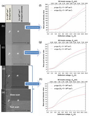
Secondary electron (SE) doping contrast in the scanning electron microscope is correlated with Fermi level pinned surfaces of Si samples prepared using HF-based wet-chemical treatment or focused ion beam (FIB) micromachining en route to quantitative dopant profiling. Using energy-resolved SE imaging techniques and finite-element analyses of surface states and surface junction potentials, we clarified the surface band-bending effects post-NH4F-treatment, consistent with brighter p-contrast from degenerately doped (>1019 cm−3) regions. In general, SE spectromicroscopy scan measurements unambiguously indicated heavy suppression of patch fields, while the empirical discovery of scan frequency-modulated contrast inversion due to Chee et al. [Springer Proceedings in Physics, 120, pp. 407–410 (2008)] is ascribable to competing fixed oxide charge and dynamic charge injection phenomena (particularly at dwell times >29 μs). Leveraging numerical simulations of electric potentials and variable-voltage experimental data, the theoretical model based on amorphization damage-mediated Fermi level pinning is elucidated for Ga+ FIB-processed site-specific doping contrast on patch field-free surfaces. This work successfully argues against the notion that doping contrast ultimately or exclusively entails patch fields or adventitious metal–semiconductor contacts.

Type
Software and Instrumentation
Copyright
Copyright © The Author(s), 2022. Published by Cambridge University Press on behalf of the Microscopy Society of America

Access options

Get access to the full version of this content by using one of the access options below. (Log in options will check for institutional or personal access. Content may require purchase if you do not have access.)

References

Allongue, P, Henry de Villeneuve, C, Morin, S, Boukherroub, R & Wayner, DDM (2000). The preparation of flat H–Si (111) surfaces in 40% NH4F revisited. Electrochim Acta 45, 45914598.CrossRefGoogle Scholar
Allongue, P, Kieling, V & Gerischer, H (1995). Etching mechanism and atomic structure of H–Si(111) surfaces prepared in NH4F. Electrochim Acta 40, 13531360.CrossRefGoogle Scholar
Alugubelli, SR, Fu, H, Fu, K, Liu, H, Zhao, Y & Ponce, FA (2019). Dopant profiling in p-i-n GaN structures using secondary electrons. J Appl Phys 126, 18.CrossRefGoogle Scholar
Angermann, H (2008). Passivation of structured p-type silicon interfaces: Effect of surface morphology and wet-chemical pre-treatment. Appl Surf Sci 254, 80678074.CrossRefGoogle Scholar
Angermann, H, Balamou, P, Lu, W, Korte, L, Leendertz, C & Stegemann, B (2016). Oxidation of Si surfaces: Effect of ambient air and water treatments on surface charge and interface state density. Solid State Phenom 255, 331337.CrossRefGoogle Scholar
Angermann, H & Henrion, W (2000). Wet-chemical passivation of Si (111)-and Si (100)-substrates. Mater Sci Eng B 73, 178183.CrossRefGoogle Scholar
Angermann, H, Rappich, J, Sieber, I, Hübener, K & Hauschild, J (2008). Smoothing and passivation of special Si(111) substrates: Studied by SPV, PL, AFM and SEM measurements. Anal Bioanal Chem 390, 14631470.CrossRefGoogle ScholarPubMed
Buzzo, M, Ciappa, M & Fichtner, W (2006). Characterization of photonic devices by secondary electron potential contrast. Microelectron Reliab 46, 15361541.CrossRefGoogle Scholar
Buzzo, M, Ciappa, M, Millan, J, Godignon, P & Fichtner, W (2007). Two-dimensional dopant imaging of silicon carbide devices by secondary electron potential contrast. Microelectron Eng 84, 413418.CrossRefGoogle Scholar
Chakk, Y, Vidoshinsky, I & Razilov, R (2007). Novel approach for visualizing implants in deep submicron microelectronic devices using dopant selective etching and low keV SEM. In Springer Proceedings in Physics, Cullis, AG & Midgley, PA (Eds.), pp. 403406. Dordrecht: Springer.Google Scholar
Chee, AKW (2016 a). Quantitative dopant profiling by energy filtering in the scanning electron microscope. IEEE Trans Device Mater Reliab 16, 138148.CrossRefGoogle Scholar
Chee, AKW (2016 b). Fermi level pinning characterisation on ammonium fluoride-treated surfaces of silicon by energy-filtered doping contrast in the scanning electron microscope. Sci Rep 6, 18. doi:10.1038/srep32003CrossRefGoogle ScholarPubMed
Chee, AKW (2018). Enhancing doping contrast and optimising quantification in the scanning electron microscope by surface treatment and Fermi level pinning. Sci Rep 8, 5247.CrossRefGoogle ScholarPubMed
Chee, AKW (2019). Principles of high-resolution dopant profiling in the scanning helium ion microscope, image widths, and surface band bending. IEEE Trans Electron Devices 66, 48834887.CrossRefGoogle Scholar
Chee, AKW (2020). Unravelling new principles of site-selective doping contrast in the dual-beam focused ion beam/scanning electron microscope. Ultramicroscopy 213, 110. doi:10.1016/j.ultramic.2020.112947CrossRefGoogle ScholarPubMed
Chee, AKW, Broom, RF, Humphreys, CJ & Bosch, EGT (2011). A quantitative model for doping contrast in the scanning electron microscope using calculated potential distributions and Monte Carlo simulations. J Appl Phys 109, 19.CrossRefGoogle Scholar
Chee, KWA, Beanland, R, Midgley, PA & Humphreys, CJ (2010). Site-selective dopant profiling of p-n junction specimens in the dual-beam FIB/SEM system. J Phy Conf Ser 209, 14.CrossRefGoogle Scholar
Chee, KWA, Rodenburg, C & Humphreys, CJ (2008 a). Quantitative dopant profiling in the SEM including surface states. In Microscopy of Semiconducting Materials 2007, vol. 120, Cullis, AG & Midgley, PA (Eds.), pp. 407410. Dordrecht: Springer.CrossRefGoogle Scholar
Chee, KWA, Rodenburg, C & Humphreys, CJ (2008 b). High resolution dopant profiling in the SEM, image widths and surface band-bending. J Phys Conf Ser 126, 14.CrossRefGoogle Scholar
Chung, MF & Haneman, D (1966). Properties of clean silicon surfaces by paramagnetic resonance. J Appl Phys 37, 18791889.CrossRefGoogle Scholar
Chung, S, Wheeler, V, Myers-Ward, R, Nyakiti, LO, Eddy, CR, Gaskill, DK, Skowronski, M & Picard, YN (2011). Secondary electron dopant contrast imaging of compound semiconductor junctions. J Appl Phys 110, 16.CrossRefGoogle Scholar
Druckmüllerová, Z, Kolíbal, M, Vystavěl, T & Šikola, T (2014). Toward site-specific dopant contrast in scanning electron microscopy. Microsc Microanal 20, 13121317.CrossRefGoogle ScholarPubMed
El-Gomati, M, Zaggout, F, Jayacody, H, Tear, S & Wilson, K (2005). Why is it possible to detect doped regions of semiconductors in low voltage SEM: A review and update. Surf Interface Anal 37, 901911. doi:10.1002/sia.2108CrossRefGoogle Scholar
El-Gomati, MM, Wells, TCR, Müllerová, I, Frank, L & Jayakody, H (2004). Why is it that differently doped regions in semiconductors are visible in low voltage SEM? IEEE Trans Electron Devices 51, 288292.CrossRefGoogle Scholar
Elliott, S, Broom, RF & Humphreys, CJ (2000). Enhanced SEM doping contrast on an H-passivated silicon surface. In 12th European Congress on Electron Microscopy, Brno, pp. 609–610.Google Scholar
Elliott, SL (2001). Dopant profiling with the scanning electron microscope. PhD Dissertation. University of Cambridge, UK.Google Scholar
Elliott, SL, Broom, RF & Humphreys, CJ (2002). Dopant profiling with the scanning electron microscope – a study of Si. J Appl Phys 91, 91169122.CrossRefGoogle Scholar
Farrell, R. M, Haeger, D. A, Fujito, K., DenBaars, S. P, Nakamura, S. & Speck, J. S (2013). Morphological evolution of InGaN/GaN light-emitting diodes grown on free-standing m-plane GaN substrates. Journal of Applied Physics 113(6), 063504. http://dx.doi.org/10.1063/1.4790636.CrossRefGoogle Scholar
Fischer, TE (1969). Determination of semiconductor surface properties by means of photoelectric emission. Surf Sci 13, 3051.CrossRefGoogle Scholar
Gonda, S, Tanaka, M, Kurosawa, T & Kojima, I (1998). Sub-nanometer scale measurements of silicon oxide thickness by spectroscopic ellipsometry. Jpn J Appl Phys 37, L1418L1420.CrossRefGoogle Scholar
Gräf, D, Grundner, M, Schulz, R & Mühlhoff, L (1990). Oxidation of HF-treated Si wafer surfaces in air. J Appl Phys 68, 51555161.CrossRefGoogle Scholar
Grundner, M & Halbritter, J (1980). On surface coatings and secondary yield of Nb3Sn and Nb. J Appl Phys 51, 53965405.CrossRefGoogle Scholar
Halbritter, J (1984). On changes of secondary emission by resonant tunneling via adsorbates. J Phy Colloq 45, 315317.Google Scholar
Higashi, GS, Becker, RS, Chabal, YJ & Becker, AJ (1991). Comparison of Si(111) surfaces prepared using aqueous solutions of NH4F versus HF. Appl Phys Lett 58, 16561658.CrossRefGoogle Scholar
Houben, L, Luysberg, M & Brammer, T (2004). Illumination effects in holographic imaging of the electrostatic potential of defects and pn junctions in transmission electron microscopy. Phy Rev B 70, 18.CrossRefGoogle Scholar
Huang, J, Loeffler, M, Moeller, W & Zschech, E (2016). Ga contamination in silicon by focused ion beam milling: Dynamic model simulation and atom probe tomography experiment. Microelectron Reliab 64, 390392. Available at http://www.sciencedirect.com/science/article/pii/S002627141630230X.CrossRefGoogle Scholar
Kazemian, P, Mentink, SAM, Rodenburg, C & Humphreys, CJ (2006). High resolution quantitative two-dimensional dopant mapping using energy-filtered secondary electron imaging. J Appl Phys 100, 17.CrossRefGoogle Scholar
Kazemian, P, Mentink, SAM, Rodenburg, C & Humphreys, CJ (2007). Quantitative secondary electron energy filtering in a scanning electron microscope and its applications. Ultramicroscopy 107, 140150.Google Scholar
Kazemian, P, Rodenburg, C & Humphreys, CJ (2004). Effect of experimental parameters on doping contrast of Si p – n junctions in a FEG-SEM. Microelectron Eng 73–74, 948953.CrossRefGoogle Scholar
Kolibal, M, Cechal, J, Bartosik, M, Mach, J & Sikola, T (2010). Stability of hydrogen-terminated vicinal Si (111) surface under ambient atmosphere. Appl Surf Sci 256, 34233426.CrossRefGoogle Scholar
Koyanagi, S, Hashizme, T & Hasegawa, H (1996). Contactless characterization of thermally oxidized, air-exposed and hydrogen-terminated silicon surfaces by capacitance-voltage and photoluminescence methods. Jpn J Appl Phys 35, 946953.CrossRefGoogle Scholar
Lederer, D & Raskin, J-P (2005). Effective resistivity of fully-processed SOI substrates. Solid-State Electron 49, 491496. https://www.sciencedirect.com/science/article/pii/S0038110104003557.CrossRefGoogle Scholar
Lin, CY & Lee, JH (2003). Enhanced SEM doping contrast. In 29th International Symposium for Testing and Failure Analysis, Santa Clara, pp. 87–89. Ohio: ASM International.CrossRefGoogle Scholar
Liu, PT & Lee, JH (2011 a). Profiling p+/n-well junction by nanoprobing and secondary electron potential contrast. IEEE Electron Device Lett 32, 868870.CrossRefGoogle Scholar
Liu, PT & Lee, JH (2011 b). Inspection of the current-mirror mismatch by secondary electron potential contrast with in situ nanoprobe biasing. IEEE Electron Device Lett 32, 14181420.CrossRefGoogle Scholar
Müllerová, Ilona, El-Gomati, Mohamed M & Frank, Luděk (2002). Imaging of the boron doping in silicon using low energy SEM. Ultramicroscopy 93, 223243. http://dx.doi.org/10.1016/S0304-3991(02)00279-6.CrossRefGoogle ScholarPubMed
Oatley, CW & Everhart, TE (1957). The examination of p-n junctions with the scanning electron microscope. J Electron 2, 568570.Google Scholar
Ouyang, JH, Zhao, XS, Li, T & Zhang, DC (2003). Direct measurement of the etching rates on Si (111) and silicon dioxide surfaces in 40% ammonium fluoride aqueous solution via atomic force microscopy. J Appl Phys 93, 43154320.CrossRefGoogle Scholar
Perovic, DD, Castell, MR, Howie, A, Lavoie, C, Tiedje, T & Cole, JSW (1995). Field-emission SEM imaging of compositional and doping layer semiconductor superlattices. Ultramicroscopy 58, 104113.CrossRefGoogle Scholar
Perovic, DD, Turan, R & Castell, MR (1998). Quantitative imaging of semiconductor doping distributions using a scanning electron microscope. In Proceedings of the International Centennial Symposium on the Electron, Cambridge 1997, Kirkland, A & Brown, PD (Eds.), pp. 258265. London, UK: IOM Communications Ltd.Google Scholar
Quadbeck, P, Ebert, P & Urban, K (2000). Effect of dopant atoms on the roughness of III–V semiconductor cleavage surfaces. Appl Phys Lett 76, 300302.CrossRefGoogle Scholar
Ramonda, M, Dumas, P & Salvan, F (1998). On the roughness of perfectly flat H–Si(111) surfaces an atomic force microscopy approach. Surf Sci Lett 411, L839L843.CrossRefGoogle Scholar
Rubanov, S & Munroe, PR (2004). FIB-induced damage in silicon. J Microsc 214, 213221.CrossRefGoogle ScholarPubMed
Salvati, E, Brandt, LR, Papadaki, C, Zhang, H, Mousavi, SM, Wermeille, D & Korsunsky, AM (2018). Nanoscale structural damage due to focused ion beam milling of silicon with Ga ions. Mater Lett 213, 346349. Available at http://www.sciencedirect.com/science/article/pii/S0167577X17316683.CrossRefGoogle Scholar
Schneider, CA, Rasband, WS & Eliceiri, KW (2012). NIH image to ImageJ: 25 years of image analysis. Nat Methods 9, 671675.CrossRefGoogle ScholarPubMed
Sealy, CP, Castell, MR & Wilshaw, PR (2000). Mechanism for secondary electron dopant contrast in the SEM. J Electron Microsc 49, 311321.CrossRefGoogle ScholarPubMed
Silvaco International Inc (2016). ATLAS User's Manual: Device Simulation Software. Santa Clara, CA: Silvaco International Inc.Google Scholar
Sutton, D, Parle, SM & Newcomb, SB (2001). Focused ion beam damage: Its characterization and minimization. In Institute of Physics Conference Series, pp. 377–381.Google Scholar
Suzuki, T & Adachi, S (1994). Chemical treatment effect of Si(111) surfaces in NH4F solution studied by spectroscopic ellipsometry. Jpn J Appl Phys 33, 55995602.CrossRefGoogle Scholar
Thornton, PR (1968). Scanning Electron Microscopy: Applications to Materials and Device Science. London: Chapman & Hall.Google Scholar
Twitchett, AC, Dunin-Borkowski, RE & Midgley, PA (2002). Quantitative electron holography of biased semiconductor devices. Phys Rev Lett 88, 14.CrossRefGoogle ScholarPubMed
Venables, D, Jain, H & Collins, DC (1998). Secondary electron imaging as a two-dimensional dopant profiling technique: Review and update. J Vac Sci Technol B 16, 362. Available at http://scitation.aip.org/content/avs/journal/jvstb/16/1/10.1116/1.589811.CrossRefGoogle Scholar
Wang, SX (2004). TEM study of surface damage and profile of a FIB-prepared Si sample. Microsc Microanal 10, 11581159. Available at http://www.journals.cambridge.org/abstract_S1431927604881315.CrossRefGoogle Scholar
Xu, L, Weber, K, Phang, SP, Fell, A, Brink, F, Yan, D, Yang, X, Franklin, E & Chen, H (2013). Secondary electron microscopy dopant contrast image (SEMDCI) for laser doping. IEEE J Photovoltaics 3, 762768.CrossRefGoogle Scholar