Hostname: page-component-848d4c4894-xfwgj Total loading time: 0 Render date: 2024-06-20T00:45:54.500Z Has data issue: false hasContentIssue false

In-situ Characterization of MoS2 Based Field Effect Transistors during Ion Irradiation

Published online by Cambridge University Press:  30 July 2020

Gregor Hlawacek
Affiliation:
Helmholtz-Zentrum Dresden-Rossendorf, Dresden, Sachsen, Germany
Zahra Fekri
Affiliation:
Helmholtz-Zentrum Dresden-Rossendorf, Dresden, Sachsen, Germany
Panish Chava
Affiliation:
Helmholtz-Zentrum Dresden-Rossendorf, Dresden, Sachsen, Germany
Artur Erbe
Affiliation:
Helmholtz-Zentrum Dresden-Rossendorf, Dresden, Sachsen, Germany

Abstract

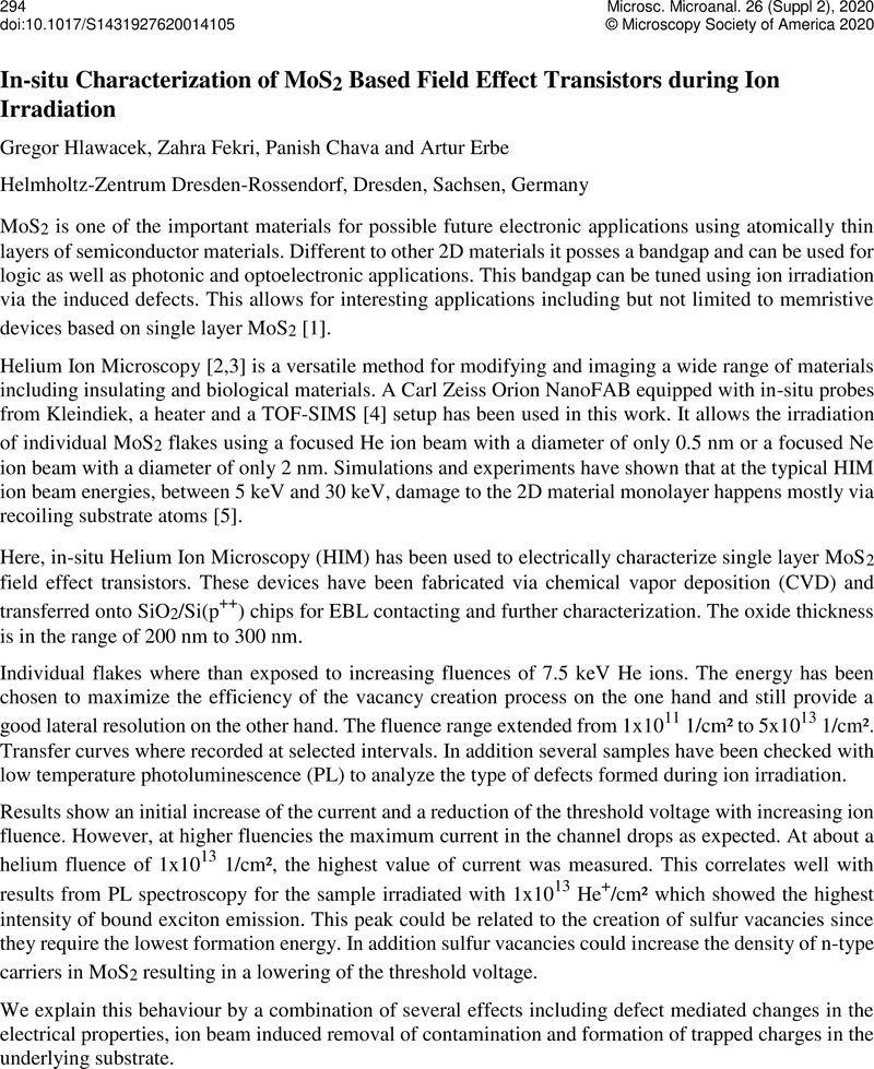
Image of the first page of this content. For PDF version, please use the ‘Save PDF’ preceeding this image.'
Type
Crystallography at the Nanoscale and MicroED with Electrons and X-rays
Copyright
Copyright © Microscopy Society of America 2020

References

Jadwiszczak, J., et al. , MoS2 Memtransistors Fabricated by Localized Helium Ion Beam Irradiation, ACS Nano 2019, 13, 1426214273.10.1021/acsnano.9b07421CrossRefGoogle ScholarPubMed
Hlawacek, G. & Gölzhäuser, A. (Eds.), Helium Ion Microscopy, Springer International Publishing, 2016.10.1007/978-3-319-41990-9CrossRefGoogle ScholarPubMed
Hlawacek, G., et al., Helium ion microscopy, Journal of Vacuum Science and Technology B, 2014, 32, 020801.10.1116/1.4863676CrossRefGoogle Scholar
Klingner, N., et al. Time-of-flight secondary ion mass spectrometry in the helium ion microscope Ultramicroscopy, 2019, 198, 101710.1016/j.ultramic.2018.12.014CrossRefGoogle Scholar
Kretschmer, S., et al. , Supported two-dimensional materials under ion irradiation: the substrate governs defect production, Applied Materials & Interfaces, 2018, 10, 3082730836.10.1021/acsami.8b08471CrossRefGoogle ScholarPubMed