Hostname: page-component-848d4c4894-wzw2p Total loading time: 0 Render date: 2024-05-08T13:33:55.685Z Has data issue: false hasContentIssue false

High Spatial Resolution Low-Voltage Electron Imaging and Spectroscopy of Two-Dimensional Materials and Semiconductor Nanostructures

Published online by Cambridge University Press:  05 August 2019

Xiaoqing Pan
Affiliation:
Department of Materials Science and Engineering, University of California - Irvine, Irvine, CA, USA. Department of Physics and Astronomy, University of California - Irvine, Irvine, CA, USA. Irvine Materials Research Institute (IMRI), University of California - Irvine, Irvine, CA, USA.
Xingxu Yan
Affiliation:
Department of Materials Science and Engineering, University of California - Irvine, Irvine, CA, USA.
Chaitanya A. Gadre
Affiliation:
Department of Physics and Astronomy, University of California - Irvine, Irvine, CA, USA.
Toshihiro Aoki
Affiliation:
Irvine Materials Research Institute (IMRI), University of California - Irvine, Irvine, CA, USA.

Abstract

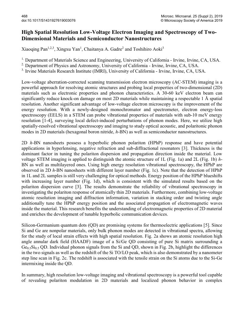
Image of the first page of this content. For PDF version, please use the ‘Save PDF’ preceeding this image.'
Type
Low Voltage, Low Energy Electron Microscopy Imaging and Analysis
Copyright
Copyright © Microscopy Society of America 2019 

References

[1]Lagos, MJ et al. , Nature 543 (2017), p. 529.Google Scholar
[2]Hage, FS et al. , Sci. Adv. 4 (2018), p. eaar7495.Google Scholar
[3]Govyadinov, AA et al. , Nat. Commun. 8 (2017), p. 95.Google Scholar
[4]Konečná, A et al. , Phys. Rev. B 98 (2018), p. 205409Google Scholar
[5]Chang, H-T et al. , Nanoscale 6 (2014), p. 3593.Google Scholar
[6]This work was supported by the Department of Energy (DOE) under Grant DE-SC0014430. The authors acknowledge the support of the University of California Irvine Materials Research Institute for the use of TEM facilities.Google Scholar