Introduction
GaN alloys have received great interest in the past decade due to applications in photonic and electronic devices. However, because of the low free hole concentrations of p-GaN (1017 cm−3) and lack of a metal with a work function ϕ equal to or greater than the bandgap plus electron affinity (Eg + χs = 7.5 eV), attempts to make low resistance ohmic contacts to p-GaN have been unsuccessful[Reference Suzuki, Kawakami, Arai, Kobayashi, Koide, Uemura, Shibata and Murakami1-Reference Youn, Hao, Sato, Sugahara, nao and Sakai12].
The purpose of this paper is to propose a general scheme by which metallization schemes for ohmic contacts can be systematically selected. The scheme is called “NOG” (Nitride-forming metal Over Gallide-forming metal) and is based on the thermodynamic stabilities of these phases during interfacial reactions between the metallization layers and the GaN semiconductor.
Principles of “NOG” Scheme
Since as-grown GaN are intrinsically n-type, there may be a high concentration of native N vacancies, VN, which is equivalent to a Ga-rich condition in the film. An opposite situation could be postulated: if a N-rich condition could be created in as-grown GaN films, the extra N atoms could create Ga vacancies and intrinsically p-GaN films However, this postulated condition might still be achieved by interfacial reactions in the contact region. If extra N atoms could be kept between the contact metal layer and the bulk p-GaN film, a N-rich condition could be formed at the metal/GaN interface. The extra N atoms could fill the VN positions and create Ga vacancies which would act as acceptors. If the Ga vacancy acceptors were sufficiently shallow and reached a high concentration, the interfacial region could become p+-GaN and current transportation could be dominated by field emission or thermionic field emission.
The principle of the “NOG” scheme is illustrated in Figure 1. A gallide-forming metal is followed by a nitride-forming metal covered with a layer of protective metal (such as Au). Under a suitable annealing condition, the gallide-forming metal would react with GaN to form stable gallides and release N atoms. This first metal layer must both dissociate the GaN lattice and prevent or slow down the process of nitrogen out-diffusion. The second nitride-forming metal would help keep the released N atoms at the contact interfacial region and create a N-rich condition.
all transition metals may be classified into three groups: the late, early and middle transition metals based on the enthalpy of the metallurgical reactions, which was called gallide-forming, nitride-forming and neutral metals in this paper. The metallurgical reaction of these metals to GaN was reported in reference [Reference Mohney and Lin13] and [Reference Mohney, Luther, Jackson and Khan14].

Figure 1. Principle of the “NOG” scheme.
Explanation of Literature
Many studies have been reported along with postulated mechanisms to explain reduced contact resistance, such as GaN re-growth [Reference Youn, Hao, Sato, Sugahara, nao and Sakai12], H extraction [Reference Suzuki, Kawakami, Arai, Kobayashi, Koide, Uemura, Shibata and Murakami1] and Ni oxidation [Reference Ho, Jong, Chiu and Chen2]. A few representative contact schemes will be discussed based on the principle of “NOG”. Other contact schemes could be analyzed similarly.
The contact scheme Ni/Au [Reference Ho, Jong, Chiu and Chen2, Reference Fung, Borton, Nathan, Hove and Hickman3, Reference Kim, Yoo and Kim4, Reference Ishikawa, Kobayashi, Koide, Yamasaki, Nagai, Umezaki, Koike and Murakami5, Reference King, Zhang, Ramer, Hersee and Lester6] is widely used for GaN device fabrication. Based on the “NOG” principles, this scheme works due to the reaction between Ni and GaN. The Ga would react with Ni to form stable gallides and reduce excess Ga atoms. Reduced excess Ga could be reflected as reduced concentration of VN.Less compensation of acceptors would result in higher free hole concentrations in the interfacial region. Other reported contact schemes like Pd/Au[Reference Kim, Lee, Lee, Shin, Park and Kim7, Reference Kim, Khim, Chae and Kim8], Pt/Au [Reference King, Zhang, Ramer, Hersee and Lester6, Reference Mori, Kozawa, Ohwaki, Taga, Nagai, Yamasaki, Asami, Shibata and Koike9, Reference Yoo, Lee, Myoung, Shim and Kim10], Pd/Au/Pt/Au[Reference Kim, Khim, Chae and Kim8], Pd/Pt/Au[Reference King, Zhang, Ramer, Hersee and Lester6] and Pt/Ni/Au[Reference Jang, Chang, Kim, Seong, Lee and Park11]contact schemes could be explained similarly.
A relatively low specific contact resistance (3.6×10⁻³ Ω-cm2) was obtained with Ni/Zn-Au [Reference Youn, Hao, Sato, Sugahara, nao and Sakai12] in p-GaN with a carrier concentration of Nh = 4.4×1017cm−3. It was postulated that Zn was an acceptor and that the Zn-Au alloy layer increased the interface carrier concentration. Zn is an acceptor, but it is deep (EA = 570 meV)[Reference Pankove and Pearton16] and therefore should not be ionized at room temperature. Based on the “NOG” scheme, the mechanism should be the same as the Ni/Au scheme discussed above. The main reason for improved contact performance probably due to the limited time for native oxide to grow on GaN and the use of high vacuum for metallization. Optimum contact resistance would not be predicted for the Ni/Zn-Au because of no nitride forming component to the metallization. The released N atoms could be released as N2 rather than kept at the interface.
A low resistivity (3.2×10⁻⁵ Ω-cm2) ohmic contact to p-GaN was produced with Ta/Ti after a high temperature anneal (800°C for 20 min) [Reference Suzuki, Kawakami, Arai, Kobayashi, Koide, Uemura, Shibata and Murakami1]. The authors postulated that Ta and Ti were able to remove hydrogen from Mg-H complexes and therefore reduced compensation of the acceptors. It was found that a dual layer structure formed better contacts than a single Ta or Ti layer. After a few days, the contact resistance increased to a much higher value. This was attributed to a reverse transport of compensating hydrogen from the Ti/Ta layers back into the interface region and recompensation of Mg acceptors. However, Fukai has reported that the enthalpy for MgH2 (−0.77 eV/atom) is more negative than for TiH2 (−0.68 eV/atom) or TaH0.5 (−0.417 eV/atom) [Reference Fukai17]. Thus for these reaction products, Ta and Ti should not reduce MgH2. In the “NOG” scheme, it would be postulated instead that Ta and Ti would dissociate the GaN and release N atoms. The released N atoms would increase the nitrogen chemical potential and result in reduced VN concentrations, in addition to forming TaNx and TiNx compounds. The differences in the thermodynamic and kinetic properties of Ta and Ti would explain why Ta/Ti form better contacts than Ta or Ti individually. The observation of an increased resistance with time at room temperature can also be explained using the “NOG” scheme since formation of stable nitrides would create VN and increase compensationof holes in the contact region.
For Ni/Mg/Ni/Si [Reference Youn, Hao, Sato, Sugahara, nao and Sakai12], contact resistance value of ≈10−3 Ω-cm2 was measured. These ohmic contacts were degraded by annealing at 500°C for 20min. The authors postulated a similar mechanism of solid phase epitaxial regrowth known to occur for AuGeNi/GaAs contacts[Reference Holloway, Kim, Trexler, Miller, Fijol, Lampert and Haas15]. The authors in the study of Ni/Mg/Ni/Si postulated that regrowth of GaN and NiSi led to ohmic contacts. Using the principles of the “NOG” scheme, formation of an ohmic contact would result from Ni dissociation of the GaN and formation of NiGax, MgNx and SiNx. The nitride phases would increase the activity of N in the interfacial region, which would create a N-rich condition and a more p-type interface. This contact metallization is close to the “NOG” scheme under discussion.
This idea of interfacial reactions and control of vacancies which is the basic tenet of the “NOG” scheme can and does apply to ohmic contact to n-GaN, not just to p-GaN. Lester, et al. [Reference Lester, Brown, Ramer, Ahang, Hersee and Zolper18] reported that aluminum produced an ohmic contact of 10−3 ohm-cm2 to n-GaN. This is reasonable because of the matched work function of Al and GaN [Reference Holloway, Kim, Trexler, Miller, Fijol, Lampert and Haas15]. The contact resistance of Al/n-GaN increased by 50% upon annealing at 575°C. The postulated reason was formation of a large bandgap AlN layer at the interface. The contact resistance was improved to 8×10⁻⁶ Ω-cm2 using a Ti/Al bilayer metals annealed at 900oC, presumably due to the formation of TiN at the interface of Ti/Al (and Ti/Al/Ni/Au) contacts [Reference Fan, Mohammad, Kim, Aktas, Botchkarev and Mokoc19, Reference Lin, Ma, Huang, Fan, Allen and Morkoc20]. Depletion of N in the GaN surface region would create more VN vacancies, and result in an n+-GaN layer with improved electron tunneling, consistent with the “NOG” scheme.
Experimental studies of Ni/Ti/Au and Ni/Al/Au
Besides analysis of published results, the “NOG” scheme was compared to experimental data collected from Ni/Ti/Au, Ni/Al/Au and Ni/Au contacts to p-GaN. Current-voltage (I-V) data showed that more current was obtained in the ternary layer contacts, consistent with predictions.
The p-GaN wafers used in this experiment were purchased from SVT Associates. The GaN 1μm epilayers were grown by MBE and had a free hole concentration of 1.1∼2.5 × 1017 cm−3. Samples were cleaned with agitated acetone (5min), methanol (5min) and boiling aqua regia (10min) sequentially before being washed with DI water. All samples were blown dry with N2 gas between each step. The contacts were deposited at a base pressure of ≈5 × 10⁻⁶ Torr.
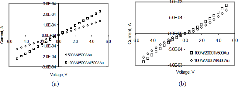
Figure 2 shows the I-V data for (a) 50nm Ni/50nm Au or 10nm Ni/50nm Al/50nm Au contacts, and (b) for 10nm Ni/200nm Ti/200nm Au or 10nm Ni/200nm Al/200nm Au. The current was a factor of two higher through Ni/Al/Au than through Ni/Au, and the current through Ni/Ti/Au was 30% higher than through Ni/Al/Au.

Figure 2 Effects of adding a nitride-forming metal to Ni/Au as-deposited contacts to p-GaN (a) Ni/Au and Ni/Al/Au; (b) Ni/Ti/Au and Ni/Al/Au
Based on the principles “NOG”, the first Ni layer in both Ni/Ti/Au and Ni/Al/Au contacts was a gallide forming metal, which would release N atoms. This Ni layer also acts as a nitride-forming barrier because of slowed N diffusion. This would maintain a higher N activity at the GaN surface, reduce VN, and result in less acceptor compenstion.
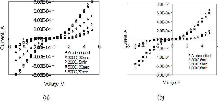
The effects of Ni thickness were studied by changing the Ni thickness (Figure 3). As the Ni changed from 2 to 10 nm the current increased by a factor of 3. A higher contact resistance for thin gallide-forming metal (2nm Ni) could result from the extent of interfacial reaction being too limited to affect VN concentration or the Ni layer is too thin to prevent quick formation of stable nitride (TiNx) and thus to increase VN concentration. The effects of annealing on Ni/Ti/Au and the Ni/Au contacts are shown in Figure 4. Both Ni/Au and Ni/Ti/Au have the same current for the as deposited samples. For Ni/Ti/Au contact, a 300°C, 30 sec anneal resulted in slightly higher current, and a 5 min anneal at 300°C resulted in a four fold increase. The current through Ni/Ti/Au contacts annealed at 300°C, 30 sec was similar to that measured for Ni/Au contacts annealed at 300°C for 5 min. After a 500°C, 5min anneal, the current though Ni/Ti/Au contacts decreased to near that of as-deposited contacts. In contrast, the current in Ni/Au contacts increased continually, even after annealing at 800°C for 30 sec. The higher as deposited current, but more serious degradation of the Ni/Ti/Au contact shows that while the nitride-forming metal (Ti) is helpful in reducing the contact resistance, it also leads to the contact instability. This would be consistent with continued reaction between Ti and N to form TiNx resulting in generation of too many VN’s.

Figure 3 Effects of Ni thickness in the as deposited Ni/Ti/Au/p-GaN contacts

Figure 4 Effects of annealing on I-V data for (a)20nmNi/50nmTi/50nmAu; (b) 50nmNi/50nmAu to p-GaN
The data in Figure 4 cannot be directly compared to those in Figure 3, since the contacts in Figure 3 are 0.5mm diameter dots defined by a shadow mask, while those in Figure 4 are a TLM pattern with a 16µm spacing defined by photolithography.
Conclusions
A new ohmic contact scheme for p-GaN called Nitride-forming metal Over Gallium-forming metals, “NOG”, was proposed and discussed. Published results for ohmic contacts to p- or n-GaN were able to be explained qualitatively by the “NOG” principles. Lower contact resistances were found for contacts with both gallide and nitride forming metals (Ni/Al/Au and Ni/Ti/Au), when compared with only a gallide-forming Ni/Au contacts.