Introduction
GaN epitaxy is commonly performed on substrates with high mismatch in both lattice parameters and thermal expansion. Whereas the first is relaxed by misfit dislocations within the first few nanometers, the latter results often in thermally induced strain of GaN epilayers as it is indicated by a variety of optical experiments [Reference Rieger, Metzger, Angerer, Dimitrov, Ambacher and Stutzmann1,Reference Shan, Hauenstein, Fischer, Song, Perry, Bremser, Davis and Goldenberg2]. Despite the known importance of thermally induced strain for GaN epitaxy, there are still a lot of open questions and uncertainties related with this subject. On the one hand, this concerns basic material parameters which are essential for a correct description of thermally induced strain in GaN layers, as the temperature behavior of the TEC of GaN in the full range from typical growth temperatures down to low temperatures of a few Kelvin as commonly used for optical experiments. Moreover, there were some indications that the TEC could depend on the characteristics of the material as the free electron concentration [Reference Leszczynski, Bak-Misiuk, Domagala and Suski3]. On the other hand, the formation of thermally induced strain in GaN epilayers in dependence on the growth procedures and parameters is far beyond to be fully understood [Reference Kisielowski, Krüger, Ruvimov, Suski, Ager, Jones, Liliental-Weber, Rubin, Weber, Bremser and Davis4].
In the present paper the thermal behavior of differently grown GaN is studied. This concerns the basic material parameters which could be investigated for bulk and homoepitaxal GaN samples of high crystalline perfection. The thermal expansion of these samples is compared to that of typical heteroepitaxial layers deposited by different growth techniques on c-plane sapphire.
Experimental
Different types of samples were investigated: bulk GaN, homoepitaxial GaN and heteroepitaxial GaN layers grown by MOCVD and MBE. The investigated GaN bulk crystals were grown at the High Pressure Research Center, Unipress, Warsaw by the high-temperature high-pressure method at 1800 K and 15 kbar [Reference Porowski5]. They have hexagonal platelet shape with lateral sizes of 3 to 4 mm. One of the bulk crystals was Mg-doped, the other was nominally undoped and overgrown by MOCVD with a 3 μm thick undoped GaN layer [Reference Weyher, Brown, Zauner, Muller, Boothroyd, Foord, Hagemann, Humphreys, Larsen, Grzegory and Porowski6]. For this, a substrate temperature of 1050°C was used similar to that applied for MOCVD of the two heteroepitaxial GaN layers deposited on c-plane sapphire. The growth conditions for these layers provided by S. DenBaars (University of California Santa Barbara) and S. Nakamura (Nichia Chemical Industries) can be found in ref. [Reference Heying, Wu, Keller, Li, Kapolnek, Keller, DenBaars and Speck7] and [Reference Nakamura, Senoh, Iwasa, Nagahama, Yamada and Mukai8]. In addition, a 4.5 μm thick GaN layer grown by MBE with an electron cyclotron plasma source on c-plane sapphire at a substrate temperature of 820°C was investigated. In contrast to the MOCVD layers, this layer was deposited directly onto the nitridated substrate without growing a low-temperature buffer before.
A high-resolution X-ray diffractometer Philips X Pert MRD equipped with a Cu sealed anode, a four crystal monochromator and a triple crystal analyzer was used for the measurements. This diffractometer was extended by a continous flow X-ray cryostat of Oxford Instruments enabling temperature dependent measurements from 10 to 630 K. The lattice parameters were calculated from the scattering angles directly measured by triple axis 2θ scans [Reference Fewster and Andrew9].
Results
The progress in the growth of GaN bulk crystals over the last few years has resulted in crystal platelets with lateral extensions of up to 10 mm characterized by very narrow X-ray diffraction profiles [Reference Porowski5] which are a prerequisite for the accurate determination of lattice parameters [Reference Fewster and Andrew9]. However, highly resolved reciprocal space maps (RSMs) for such crystals as shown in figure 1 for an overgrown GaN substrate indicate that even the small GaN crystals obviously can consist of several macroscopic grains. Within the area of about 1 mm2 illuminated by the X-ray beam, we found typically two or three grains contributing to the scattered signal as indicated by corresponding sharp intensity maxima in the (00l) RSMs at different qx values. From the difference in qx the tilt of the crystallographic orientation between different grains can be calculated to be in the range of a few hundred arcseconds. Additionally, the grains are characterized sometimes by slightly different lattice parameters as it is indicated by the small shift of the intensity maxima A and B along qz in figure 1. The changes in lattice parameter c by 8·10−4 Å between different grains can be ascribed to different impurity concentrations pointing to a possible preferential accumulation of impurities in some grains.

Figure 1. Triple axis 2θ/ω scan for the (006) reflection (a) and the corresponding RSM (b). The intensity maximums A and B are assigned to two grains of the substrate with different lattice parameter c.
The composition of the GaN bulk crystals of several grains with possibly slightly different lattice constants requires special efforts for an accurate determination of the temperature behavior of GaN lattice parameters. In our experiments, RSMs and triple axis ω scans were performed before measuring the scattering angle by 2θ/ω scans. In this way it was ensured that the lattice parameters of the same grain were determined at all temperatures.
The RSM in figure 1(b) clearly demonstrates that the grain structure of the GaN substrate is reproduced in the overgrown layer as expected. The shift of substrate and layer intensity maxima along the qz axis corresponds to a difference in c lattice parameter of 2·10−3 Å. In earlier reports this behavior was ascribed to native defects or to different free electron concentrations in substrate and layer material [Reference Leszczynski, Bak-Misiuk, Domagala and Suski3]. RSMs of asymmetric reflections showed the pseudomorphic state of the layer in the whole temperature range investigated.
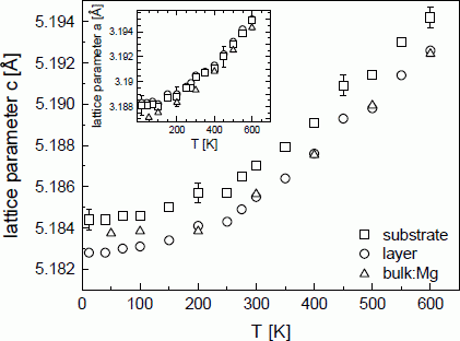
The lattice parameters of homoepitaxial layers and GaN bulk crystals come close to each other if the bulk material is Mg doped during growth [Reference Porowski5]. This is confirmed by figure 2 where the lattice parameters c of the intentionally undoped GaN bulk, the homoepitaxial layer deposited on it, and a Mg doped GaN crystal are plotted in dependence on the temperature.

Figure 2. Lattice parameters c in dependence on the temperature for an undoped bulk crystal (substrate) overgrown with a 3 µm thick MOCVD layer and a Mg-doped GaN bulk crystal. The error bars are representative for all lattice parameters given. The lattice parameters a are shown in the inset.
Similarly to the GaN bulk and the homoepitaxial layer, several μm thick heteroepitaxial GaN layers on sapphire substrates were investigated. In figure 3 the results for the c lattice parameters of layers grown by MOCVD and MBE are compared with those for the GaN bulk material and the homoepitaxial layer. For better clarity the latter data are represented as lines. Clear differences are visible for the two MOCVD samples. Whereas the sample MOCVD II has a c lattice parameter which is clearly higher than that of the homoepitaxial layer in the whole temperature range, the c values from the MOCVD I sample are near to those of the homoepitaxial layer. For the MBE grown layer the lattice parameters are between those of the MOCVD samples. Obviously, the slopes of the curves differ clearly for the different samples as well.

Figure 3. Comparison of the lattice parameters c in dependence on the temperature for bulk GaN, homoepitaxial and different heteroepitaxial GaN layers.
Discussion
From figure 2 the following informations can be obtained: (1) The temperature dependence of thermal expansion of GaN can be extracted. This has been done in ref. [Reference Wang and Reeber10] assuming a linear expansion within each of the temperature ranges of 10 to 100 K, 100 to 250 K, and 250 to 600 K. (2) Within the experimental errors, there is no indication for negative TEC at low temperatures. However, the amount of negative TEC as reported for other materials is often too small to be reflected in a significant change in lattice constants [Reference Wang and Reeber11]. (3) The difference in lattice parameters between the homoepitaxial layer and the underlying substrate is constant over the whole investigated temperature range with an accuracy of 2·10−4 Å.
The differences in c lattice parameters for the heteroepitaxially grown layers can be partially attributed to different growth temperatures for the MOCVD and the MBE process. Since the growth temperature for the MOCVD samples is higher than that for the MBE sample, the thermal strain induced in the MOCVD layers should be higher. This is obviously the case for the MOCVD II sample for which the larger lattice parameters in growth direction indicate a stronger compressive biaxial strain. For the MOCVD I sample this model fails because the strain state seems to be the same as that of the MBE sample. A comparison of the a lattice parameters (not shown here) indicates that this is probably due to large hydrostatic strain components in the MBE and MOCVD I sample.
The increase of the lattice parameters c for all three heteroepitaxial layers is different from that of the bulk crystals and the homoepitaxial layer. Below 200 K the slope is close to zero as for the bulk and homoepitaxial GaN, but above 200 K the slope is clearly smaller than for the bulk material. This reflects directly the thermally induced strain in the epilayers grown on sapphire. On the other hand, the crossing of the curves for the heteroepitaxial layers with those for the bulk material far below the growth temperatures points to a strong influence of compressive hydrostatic strains in these layers.
Summary
The temperature dependence of the lattice parameters of bulk, homoepitaxial and heteroepitaxial GaN was investigated and compared. Neither an influence of the electron concentration on the thermal expansion nor a negative thermal expansion at low temperatures was found in our experiments for bulk and homoepitaxial GaN. The comparison of results for heteroepitaxial samples with bulk values points to a superposition of thermally induced biaxial strain and compressive hydrostatic strain in the heteroepitaxial layers.
Acknowledgements
The authors would like to thank I. Grzegory and S. Porowski (High Pressure Center, Unipress, Warsaw) for the growth of the GaN single crystals and P. Prystawko for the MOCVD growth of the GaN homoepitaxial layer. The heteroepitaxial MOCVD layers were generously provided by S. DenBaars (University of California Santa Barbara) and S. Nakamura (Nichia Chem. Ind.) which is kindly acknowledged.