facets. The a type dislocations are found to fold many times from basal to the prismatic plane, whereas when a+c dislocations bend to the basal plane, they were not seen to come back to a prismatic one.
Introduction
The epitaxial lateral overgrowth (ELO) technique has proven to be a relevant process to decrease the dislocation densities from 10 10 to less than 10 7 cm −2 in GaN layers grown on sapphire. It has been implemented in both Metalorganic Vapor Phase Epitaxy (MOVPE) [Reference Kapolnek, Keller, Vetury, Underwood, Kozodoy, Denbaars and Mishra1-Reference Marchand, Wu, Ibbetson, Fini, Kozodoy, Keller, Speck, DenBaars and Mishra3] and Hybrid Vapor Phase Epitaxy (HVPE) [Reference Usui, Sunakawa, Sakai and Yamaguchi4, Reference Sakai, Sunakawa and Usui5], and considerable attention has been focussed on it, since a blue laser diode grown on an ELO GaN substrate, resulted in a lifetime of more than 10000 hours [Reference Nakamura, Senoh, Nagahama, Iwasa, Yamada, Matsushita, Kiyoku, Sugimoto, Kozaki, Umemoto, Sano, Chocho and Hiramatsu6]. The conventional ELO method can be described as follows: first, a GaN layer of a few micrometers thick is grown, then a dielectric (SiO2 or SixNy) mask is deposited. Using standard photolithographic techniques, stripes are opened in the mask. During regrowth, either by MOVPE or HVPE, growth only occurs in the openings i.e., selective area epitaxy is achieved. A lateral growth over the mask leads to full coalescence. A smooth surface suitable for device fabrication is obtained if the ratio of the lateral to vertical growth rates is high enough. The standard way to realize ELO is to induce the lateral growth from the very beginning of the regrowth process[Reference Beaumont, Vaille, Nataf, Bouillé, Guillaume, Vennéguès, Haffouz and Gibart7]. Whereas the misfit between GaN and 6H-SiC is 3.5% instead of 16% on sapphire. The epitaxial layers have similar defect densities on both substrates. This effect has until now been attributed to the mosaïc growth of GaN on these substrates, with slightly misoriented islands bounded by threading dislocations. The lattice mismatch between AlN and 6H-SiC is about 1% which makes it most adequate as a buffer layer for the growth of GaN. In the following, we investigate the possibility of using HVPE AlN and 2S-ELO GaN in order to improve the quality of the active layers.
Experimental
Prior to epitaxy, the SiC was chemically cleaned and then H2 plasma treated, then a 100nm Al buffer layer was deposited by HVPE at 1100°C. The growth of GaN was next performed in a homemade MOVPE vertical reactor operating at atmospheric pressure. The carrier gas used in this study is a mixture of H2:N2. Trimethylgallium (TMGa) and NH3 are used as precursors. A HeNe laser reflectometry set-up is used to monitor in-situ the growth process. First a 2μm-thick GaN layer is deposited directly on sapphire. In order to have large areas with electron transparency, it was necessary to prepare TEM samples by the tripod method. In this technique, two specimens are glued face to face using epoxy for cross section preparation. Then the first face is polished using a series of diamond coated plastic discs down to 0.5nm granulometry followed by silica colloïdal 0.05nm solution. Then 0.5 to 1nm slab is cut and glued on the tripod in order to grind the second face down to electron transparency. During this step, the thickness is monitored by use of silicon as one of the slabs. Therefore, when the sample thickness comes down to 10 μm, silicon becomes transparent and the polishing is stopped when the thickness fringes cross the interface and extend into the area of interest. In this process, the silicon is used to protect the specimen under study and is completely eliminated in the final stage of polishing. Usually a short cleaning in the ion mill is necessary before examination in the microscope. The specimens were analysed using a Jeol 2010 electron microscope operating at 200 kV.
Results
At the initial stage of ELO, the use of circular windows has allowed us to determine the directions of fastest growth. Coalescence is only starting and the flat top islands are faceted (Figure 1a). In the Laue pattern, the mirror
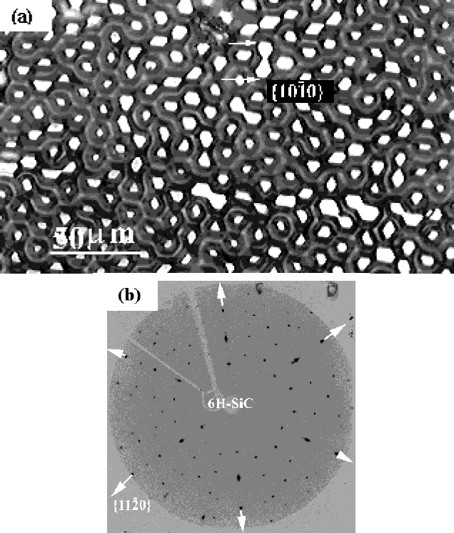
Figure 1: Surface morphology of the islands obtained by ELO during the first stage of growth (a), as well as the orientation of the surface (b).
As seen on figure 2, the use of a tripod allows to have a transparent area which extends to more than 100nm; this was used to investigate the various areas of the pyramidal islands. In particular, a simple diffraction experiment confirms the Laue orientation of figure 1 and shows that the interfaces between adjacent pyramids are along vertical

Figure 2. A TEM specimen of GaN obtained by the tripod polishing method
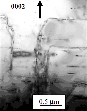
In particular a detailed analysis of the bending of dislocations has been carried out. From the center of the island, it can be seen in the 0002 dark field images that all the dislocations with c and a + c Burgers vectors bend to the basal plane (Fig. 3). Once this bending is accomplished, the dislocation will definitely stay in the basal plane.

Figure 3. A 0002 weak beam image showing the bending of threading dislocations which have a c component in their Burgers vectors.
In the case of edge type

Figure 4. A
Conclusion
In this work, we have shown that the threading dislocations bend to the basal plane on top of HVPE AlN on SiC. Based on these results and those available in the literature, it may be concluded that the lateral epitaxy is not a substrate driven mechanism. It is a consequence of the anisotropy of the properties of the crystals, such as dependence of the growth velocity on the crystallographic directions. Moreover, it is shown that the dislocation behavior is probably dependent on their Burgers vector. However more work is still needed in order to be able to make a more definite conclusion.