Introduction
(GaIn)(AsN) alloys grown on GaAs substrates offer the unique possibility to realize optoelectronic devices for the wavelength emission in the range of 1300-1550 nm due to the large band gap bowing [Reference Bellaiche, Wie and Zunger1,Reference Sakai, Ueta and Terauchi2]. In particular, the realization of vertical-cavity surface-emitting lasers (VCSEL) emitting in the 1.3µm wavelength range at room temperature [Reference Ellmers, Höhnsdorf, Koch, Agert, Leu, Karaiskaj, Hofmann, Stolz and Rühle3], solar cells in the 1.0-1.2 µm range [Reference Kurtz, Allerman, Jones, Gee, Banas and Hammons4] and resonant-cavity-enhanced (RCE) photodetectors operating near 1.3µm [Reference Heroux, Yang and Wang5] was demonstrated recently. However, this material system exhibits a large miscibility gap under thermodynamic equilibrium conditions. Therefore, extreme non-equilibrium conditions at low growth temperatures are required in order to maintain homogeneous epitaxial deposition for the metastable (GaIn)(NAs) material system.
Due to the large miscibility gap of (GaIn)(AsN) the understanding of phase separation effects, as observed in Ga(AsN) and In(AsN) [Reference Behbehani, Piner, Liu, El-Masry and Bedair6,Reference Beresford, Stevens and Schwartzman7], is of great importance. Phase separation effects lead to large local strain fields and might be the origin of 3d-like quantum dot growth [Reference Xin, Kavanagh, Zhu and Tu8].
In this work, we investigate the structural properties of (GaIn)(AsN)/GaAs MQWs grown at low temperature (525°C) by metalorganic vapour phase epitaxy (MOVPE) using triethylgallium (TEGa), trimethylindium (TMIn), tetriarybutylarsine (TBAs) and 1,1-dimethylhydrazine (UDMHy). The structural properties were investigated by means of high-resolution x-ray diffraction (HRXRD), secondary ion mass spectrometry (SIMS) and transmission electron microscopy (TEM).
Growth and Characterization
The (GaIn)(AsN)/GaAs multiple quantum well (MQW) heterostructures were grown by metal-organic vapor-phase epitaxy using an IR-heated horizontal reactor system (Aix 200). Triethylgallium (TEGa) and trimethylindium (TMIn) have been used as group-III sources and tetriarybutylarsine (TBAs) and 1,1-dimethylhydrazine (UDMHy) as group-V precursors. The growth was performed at a reactor pressure of 50 mbar under H2 carrier gas at a total flow of 6800 sccm. All the samples here investigated were grown at the same temperature (525°C) on [100]-oriented GaAs substrates. The growth rates of the quaternary (GaIn)(AsN) wells and the GaAs barrier layers were 0.25µm/h and 1.0µm/h , respectively. In order to avoid strain relaxation processes and the generation of associated structural defects, the total thickness of the MQW structures was chosen to be smaller than the critical thickness, i.e. the MQWs consist of only 5 periods. The nominal thickness of the GaAs barriers and the quaternary (GaIn)(AsN) wells are the same for all the samples investigated, i.e. db=90nm and dw=10nm, respectively. The growth parameters were optimized in order to have an In-content of x=0.33 in the quaternary layers. The N-content is constant in the individual well layers of one sample but it varies for the different samples of the investigated series in the range of y=0.01 and y=0.045.
The x-ray diffraction experiments were performed by using a high-resolution multi-crystal x-ray diffractometer. A 4-crystal channel-cut monochromator-collimator arrangement has been used to reduce the wavelength and angular dispersion of the beam incident on the sample, which are for the CuKα-radiation used 2.5×10⁻⁵ and 60µrad, respectively. The experimental x-ray diffraction patterns were simulated by using a dynamical scattering model in the recursive formalism [Reference Tapfer, Ospelt and von Känel9]. The second-order approximation of the angular deviation was used in order to obtain precise values of the lattice strain [Reference Tapfer, De Caro, Giannini, Schönherr and Ploog10].
High quality specimens for TEM experiments were prepared in [011] cross-section geometry by using mechanical pre-thinning and subsequent ion-milling (3.5-4.5 keV Ar ions) at liquid nitrogen temperature in order to minimize ion-induced damage and artefacts [Reference Barber11]. In particular , the use of a cooled stage specimen holder prevents the eventual element interdiffusion due to the local increases of the temperature during ion bombardment. The TEM specimens were analyzed by using a Philips CM30 TEM/STEM electron microscope operating at 300 keV with an interpretable resolution limit of 0.23nm. The micrographs were acquired digitally by using a Gatan 1024×1024 slow scan CCD camera.
SIMS analysis was carried out on a CAMECA ims 4f instrument using either a 2.5 keV O2 + or a 5.5 keV Cs + ions, with off-normal impacting angles of 55° ( 2 keV ), and 42° (5.5 keV), respectively. The different conditions were chosen in order to improve the depth resolution, to better detect the indium and nitrogen signal and to reduce the matrix effects. The primary beam currents were chosen in the range of 20-60nA. The secondary ions were collected through an aperture which delimited the analyzed area to a section of 8µm diameter in the center of the eroded area (a square with a side of 250µm). Positive single ionized species were monitored under oxygen bombardment while molecular ion clusters MCs + (M=Ga, In, As, N) were detected when the cesium beam was employed [Reference Gerardi, Giannini, Passaseo and Tapfer12]. The erosion rate was estimated by measuring the sputtered depth in the different matrices by using a stylus profilometer (TENCOR-alphastep).
Experimental Results and Discussion
All the MQW samples ( series of 6 samples) were analyzed in detail by HRXRD, SIMS and TEM. Here, for brevity sake we report on the results obtained on one selected sample which are representative for the whole series.
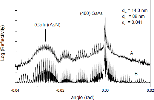
The HRXRD patterns close the (400) reciprocal lattice points of all the MQWs with different N-content exhibit a broad diffraction peak at lower angular position, about 20-30 mrad far from the GaAs substrate peak, which can be attributed to the quaternary (GaIn)(AsN) layers (see curve A of figure 1). This assumption is confirmed by kinematical simulation of the diffraction pattern and will hold if the well thickness is much smaller than the barrier thickness, i.e. dw<<db. Consequently, the angular position between the quaternary layer peak and the GaAs substrate peak is related to the lattice strain in the (GaIn)(AsN) layers. The quaternary layers of all the samples here investigated are compressive-strained. In addition, the width of the quaternary layer peak is related to the thickness of the individual well layers in the sample. The high frequency interference fringes are due to finite thickness of the MQW and the fringes angular distance is related to the whole MQW thickness. The appearance of these interference fringes indicates a high structural quality and thickness homogeneity of the heterostructures. This evidence is also confirmed by additional measurements close to the (200) and asymmetric (422) and (511) diffraction peaks. In fact, the results of these measurements demonstrate that the heterostructures are in a pseudomorphic state, i.e. the in-plane strain is zero.
Figure 1 shows the experimental (curve A) and dynamically (curve B) simulated x-ray diffraction pattern of the selected MQW. The experimental curve is shifted with respect to the simulated one for clarity sake. The following parameters were used for the best simulation pattern: the well and barrier thickness are dw=14.3nm and db=89nm, respectively, and the lattice strain along the [100] direction is ε⊥=0.041.

Figure 1 Experimental (A) and simulated (B) (400) HRXRD pattern of the MQW considered.
Unfortunately, the In and N concentration cannot be obtained from x-ray scattering experiments alone. The strain field depends on the In- as well as N-content and in addition, if the N-content is small (<30%) the influence on the structure factor will also be very small or experimentally not detectable. The incorporation behavior of In and N for the novel (GaIn)(AsN) metastable material system is very complex in MOVPE growth and not fully understood yet. However, if we assume that the In incorporation is independent from the N-incorporation [Reference Xin and Tu13], we will obtain for pseudomorphic layers of lattice strain ε* the following relation between xIn and yN:

Here, aj is the bulk lattice constants of material j and ν is the Poisson ratio of GaAs. For In-concentration xIn=0.33, as estimated from the growth parameters used for the samples investigated here, we obtain the N mole fraction yN=0.015. However, it is important to note that there are indications that the incorporation of In and N are interdependent [Reference Pan, Miyamoto, Schlemker, Sato, Koyama and Iga14]; in this case equation (1) should be used with care.
The In- and N-distribution as well as eventual segregation or interdiffusion of In and N in the MQWs were measured by SIMS. Figure 2 shows the SIMS profiles of sample A by using MCs+ 5.5keV ions (a) and O2 + 2.5 keV ions (b). The O2 + measurements allow a higher spatial resolution but are affected by a much stronger matrix effect. The results clearly show that N is localized in the quaternary layers and the N-signal is constant for all the 5 layers in the MQW. The In-concentration is the same for all the 5 well layers and no interdiffusion or segregation phenomena can be revealed [Reference Gerardi, Giannini, Passaseo and Tapfer12]. These results are also confirmed by SIMS measurements carried out on the other samples.

Figure 2 SIMS profiles obtained by using 5.5keV Cs+ (a) and O2 + (b) primary beam.
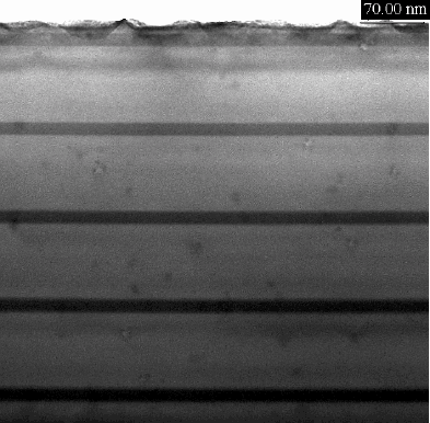
A deeper insight in the structural properties of the MQWs and the local structure of the (GaIn)(AsN)/GaAs interfaces has been obtained by TEM analyses. Figure 3 shows a bright field (BF) image of the sample A. The 5 (GaIn)(AsN)/GaAs periods are well observed and are uniform in thickness. The diffraction condition is chosen in order to minimize the crystallographic contrast and to show the quaternary layers darker with respect to the GaAs ones. The layer closer to the sample surface are brighter due to the decrease of the TEM specimen thickness and due to the related decrease of the high energy electron absorption in the relevant area. A relatively low density of extended defects has been observed. In particular, dislocations have been observed in the (GaIn)(AsN) layers with an average spacing of about (2±1) µm along the [011] cross section geometry. These dislocations are probably caused by the high lattice strain in the quaternary layers as measured by x-ray diffraction and are less frequent in layers of lower mismatch and smaller thickness.

Figure 3 BF image of the considered sample showing all the layers of the MQW.
Figure 4 is a high-resolution TEM micrograph in [011] zone axis of a (GaIn)(AsN) well shown in figure 3. The GaAs/(GaIn)(AsN) interfaces are sharp while the (GaIn)(AsN)/GaAs interfaces are slightly rougher. Similar asymmetric roughness profiles were also observed in (GaIn)As/GaAs multilayers [Reference Chao, Liu, Shih, Gotthold and Streetman15]. The roughness of the (GaIn)(AsN)/GaAs interfaces may also explain (i) the tail in the In-concentration at the (GaIn)(AsN)/GaAs interfaces as obtained by O2 + SIMS profiling (figure 2b), and (ii) the reduced amplitude of the interference fringes modulation in the high-resolution x-ray diffraction measurements (figure 1). It is also important to note that no clustering phenomena could be observed by TEM in the samples investigated here.

Figure 4 HRTEM image of one (GaIn)(AsN) layer of the MQW shown in figure 3.
Conclusions
In summary, the structure of compressive strained (GaIn)(AsN)/GaAs MQWs grown by MOVPE was investigated by using HRXRD, SIMS and TEM. We show that (GaIn)(AsN) layers of high structural quality can be fabricated up to lattice mismatches of 4%. We found that N and In atoms are localized in the quaternary material and no evidences of In-segregation or N-interdiffusion could be found. TEM analyses reveal a low defect density in the highly strained layers, but no clustering or interface undulation could be detected. High-resolution TEM images show that (GaIn)(AsN)/GaAs interfaces are slightly rougher than GaAs/(GaIn)(AsN) ones.
Acknowledgements
The financial support of the Volkswagen-Stiftung (Hannover, Germany) is gratefully acknowledged.