


1. Introduction
Recent developments of III-V nitrides has extended their applications greatly in the areas of electrical devices as well as optical devices. The use of III-V nitrides on electrical devices is beneficial from their high breakdown voltages due to the wide band-gap, and high electron velocities. After the first demonstration of Heterojunction Field Effect Transistors (HFET's) on III-V nitrides Reference Khan, Kuznia, Bhattarai and Olson[1], high power Reference Khan, Shur, Chen, Burm, Schaff, Chu and Eastman[2] and high frequency devices Reference Khan, Kuznia, Olson, Schaff, Burm and Shur[3] have developed. Current state of the art transistors on III-V nitride materials have achieved transconductances of 120 mS/mm Reference Morkoç[4] or more and current densities in excess of 600 mA/mm Reference Khan, Shur, Chen, Burm, Schaff, Chu and Eastman[2]. For microwave devices, current gain cut-off frequency, ft, of 32.1 GHz Reference Khan, Chen, Shur, Dermott, Higgins, Burm, Schaff and Eastman[5] and maximum oscillation frequency, fmax, of 77.5 GHz Reference Burm, Schaff, Eastman, Amano and Akasaki[6] have been reported utilizing 0.25 μm gate, and even higher ft and fmax have been achieved Reference Khan, Shur, Chen, Burm, Schaff, Chu and Eastman[2]. Employing III-nitride layers, Metal-Semiconductor Field Effect Transistors Reference Khan, Kuznia, Bhattarai and Olson[1] Reference Binari, Rowl, Kelner, Kruppa, Dietrich, Doverspike and Gaskillin[7], Metal-Insulator Field Effect Transistors Reference Binari, Rowl, Kelner, Kruppa, Dietrich, Doverspike and Gaskillin[7], and Modulation Doped Field Effect Transistors (MODFET's) have been fabricated.
2. Fabrication
The MODFET layers are grown by organometallic vapor phase epitaxy (OMVPE) on a (0001) Sapphire substrate. The grown layers are, from the bottom, an AlN buffer layer, thick (3-5 μm) GaN layer, 200 Å Al0.16Ga0.84N layer, 75 Å GaN channel, 50 Å Al0.16Ga0.84N spacer, 20 Å Si doped Al0.16Ga0.84N charge supply layer, 130 Å Al0.16Ga0.84N barrier, and 60 Å Al0.06Ga0.94N cap layer. The charge supply layer and cap layer were Si-doped with a doping density of 2×1018cm− 3(Figure 1) Reference Burm, Schaff, Eastman, Amano and Akasaki[6]. A Hall Measurement from Van der Pauw configuration showed a mobility of 680 cm2/Vs and a sheet charge density of 7.3 × 1012cm−2 at room temperature.
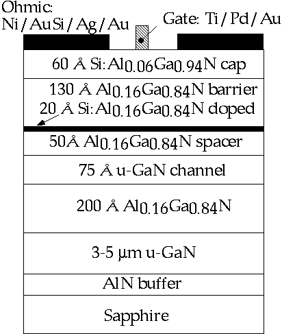
Figure 1. MODFET layer structure
On the wafer, MODFET's were fabricated. Ni/AuSi/Ag/Au (100 Å/1000 Å/1000 Å/1500 Å) was used for ohmic contacts and was annealed at 750°C for 30 s under N2 atmosphere. The contact resistance was measured from a separate transmission line model (TLM) patterns to be 9.2 Ωmm. For the device isolation, proton (H+) bombardment was used Reference Khan, Kuznia, Bhattarai and Olson[1]. The penetration depth of protons was on the order of 1.0 μm. Electron-beam lithography was used to define 0.25 μm gates, and Ti/Pd/Au was employed as the gate metal. Before evaporating gate metals, the sample was cleaned with Buffered Oxide Etch to remove any oxides formed. Ti is known to have a Schottky barrier height of 0.58 eV on GaN from the measurement by Binari et al. Reference Binari, Dietrich, Kelner, Rowland, Doverspike and Gaskill[8]. The gate width of the MODFET's was 100 μm.
3. Measurements and Discussions
On fabricated MODFET's, DC characteristics as well as RF characteristics were measured. A drain current of 150 mA/mm was reached at 0 V gate bias (Figure 2a). The peak transconductance was 40 mS/mm (Figure 2b). The series source and drain resistances determined from the voltage divider measurement technique Reference Reeves and Harrison[9] were 14.6 Ωmm and 16.5 Ωmm respectively. The high contact resistances limited the device performance. The intrinsic transconductance calculated from the measured extrinsic conductances of 40 mS/mm was 96 mS/mm. From the gate length of 0.25 μm, the effective gate length can be calculated by adding twice the distance from gate to 2 dimensional electron gas. The calculated effective gate length is 0.31 μm. For the MODFET's, HP8510 network analyzer was used to measured S-parameters for the frequency range from 45 MHz to 26.5 GHz. The cutoff frequency, ft, and maximum oscillation frequency, fmax were determined from the current gain (h21) and Mason's Unilateral gain (U), respectively. At a drain bias of 24 V, ft of 21.4 GHz and fmax of 77.5 GHz were obtained (Figure 3). The increase of the drain bias caused the increase of ft and fmax to a certain bias. This increase is currently believed to be from the composite effects of the increase of transconductance, according to the gradual channel model, and the decrease in the gate-drain capacitance, Cgd, with the drain bias increase as pointed out by Tasker et al Reference Tasker and Hughes[10].
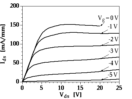
Figure 2a. Current-Voltage Characteristics of a MODFET.

Figure 2b. Transconductance (gm) and drain current (Ids) of a MODFET.
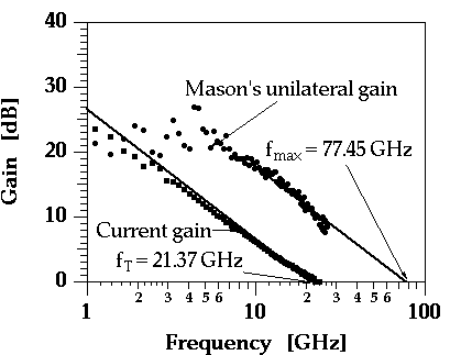
Figure 3. ft of 21.4 GHz and fmax of 77 GHz was obtained at the drain bias of 24 V.
A simple analytical method can be used to solve for the electron sheet density, N s , in a full thin quantum well, using delta-doping, an Al0.4Ga0.6N barrier with a minimum of 0.12 V above the Fermi energy, and 0.15 V ground state for electrons in the 30 Å In0.25Ga0.75N channel. The following equations apply.
where
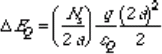

In the equation , ΔE c(2a)=3 nm, the thickness of the quantum well, ε Q is the dielectric constant of the quantum well (12.77 ε o ), q is the electronic charge, W s =5 nm, the thickness of the spacer layer, and ε s is the dielectric constant in the spacer (11.0 ε o ). The quantum well state density is 88x1012/cm2-V. For this single-sided doping case, solving the equation yields N s ≅ 7.3 × 1012 cm−2. For double-sided doping, ΔE Q is a quarter of the above, while ΔE s is one half of the above. In this double-sided doping case, N s ≅ 1.4 × 1013 cm−2. ΔE s is the potential change in the quantum well, due to an assumed uniform charge density of (N s /2a, and ΔE s is the potential change in the spacer layer due to the associated electron charge of qN s for single-sided doping, or (qNs /2) for double-sided doping. This simple solution assumes that there is a nearly constant potential in the quantum well, equal to (2/3)ΔE Q . The results of these simple calculations agree within ~10%, with the dedicated quantum mechanical solution of N s .
4. Conclusion
A III-V nitride modulation doped field effect transistor structure was employed to fabricate FET's. The OMVPE grown wafer included a 75 Å GaN channel, a 50 Å Al0.16Ga0.84N spacer and a 130 Å Al0.16Ga0.84N barrier. The Si doped charge supplying layer was confined in 20 Å. The MODFET's were fabricated using proton bombardment for isolation, with Ni/AuSi/Ag/Au ohmic metal, and Ti/Pd/Au gate metal. The 0.25 μm × 100 μm gate devices yielded a maximum transconductance of 40 mS/mm and a drain current of 150 mA/mm at 0 V gate bias. RF results revealed ft of 21.4 GHz and fmax of 77.5 GHz at the drain bias of 24 V. A simple analytical method can be useful in designing these structures to yield electron sheet density values.
Acknowledgments
The authors wish to thank Glenn H. Martin, William Davis, and Tyler Eustis for helpful discussions. The work at Cornell University is supported by the Office of Naval Research of U.S.A. (Contract No. N00014-95-1-0926). The work at Meijo University was partly supported by the Ministry of Education, Science, Sports and Culture of Japan (Contract Nos. 07505012 and 07650025).


