Introduction
Strain plays an important role for group-III nitride materials because of large lattice mismatch between binary alloys, and most substrate materials available so far [Reference Orton1]. A possible way to overcome difficulty in growth of high-quality GaN/Al x Ga1− x N heterostructures may be the growth of superlattice (SL) structures with few Angstrom periods. Such SL’s may be highly strained. If the SL period remains within the critical thickness of the SL constituents, the stacked {GaN}-{Al x Ga1− x N} sublayers should form tensile and compressive stressed “barriers” and “wells” within the SL, and adopt a common in-plane lattice constant. Besides strain-induced shift of SL phonon modes and band-gap energies, the Al x Ga1− x N sublayers should act as barriers and confine free carriers to the GaN sublayers. These carriers should then behave similarly to a two-dimensional carrier gas because of the mobility confinement perpendicular to the SL interfaces. Gleize et al. have recently studied a strained GaN-AlN-SL with average Al concentration of 48% using µ-Raman investigations [Reference Gleize, Demangeot, Frandon, Renucci, Widmann and Daudin2]. The SL was grown by mole-cular beam epitaxy. The authors observed strain-induced shifts of the GaN-sublayer phonon modes, but no free-carrier effects were detected. An estimate for the in-plane strain, ∊ xx , and the average biaxial stress, σ xx , was given using elastic constants (Cij ), and phonon deformation potential constants (a λ, b λ) for α-GaN given in Refs. [Reference Polian, Grimsditch and Grzegory3] and [Reference Davydov, Averkiev, Goncharuk, Nelson, Nikitina, Polkovnikov, Smirnov, Jacobson and Semchinova4], respectively.
Spectroscopic ellipsometry (SE) is known to be an excellent technique for measurement of thin-film optical properties. Successful application of infrared (IR) SE for measurement of phonon and free-carrier effects in group-III nitride heterostructures was reported previously [Reference Schubert, Kasic, Tiwald, Off, Kuhn and Scholz5,Reference Kasic, Schubert, Einfeldt and Hommel6]. SE is an indirect technique, and calculated model spectra need to be fit to experimental data. If appropriately chosen, model parameters, which parameterize the dielectric functions of the sample constituents, can provide physically meaningful quantities, such as transverse-optical (TO), longitudinal-optical (LO) frequencies and broadenings, static or high-frequency dielectric constants, and layer thickness. Because free-carrier absorption affects the IR dielectric response, concentration and mobility parameters can be extracted from the IRSE lineshape analysis if the carrier effective mass is known [Reference Tiwald, Woollam, Zollner, Christiansen, Gregory, Wetteroth, Wilson and Powell7]. When combined with electrical Hall measurements, the IRSE data can further provide information about the effective mass parameter, as recently demonstrated for n- and p-type α-GaN [Reference Kasic, Schubert, Einfeldt and Hommel6].
The focus of this work is to investigate stress and free-carrier effects in a strained α-GaN-AlN-SL by measurement of the long-wavelength dielectric response using IRSE for the first time, in combination with µ-Raman investigations.
Experimental
One SL with 16 periods of alternating wurtzite GaN (8 nm) and AlN (3 nm) layers was grown by MOVPE on (0001) sapphire. A 1-µm-thick GaN layer was deposited on a ∼15 nm AlN buffer layer prior to the SL (for more details see Ref. [Reference Scholz, Härle, Bolay, Steuber, Kaufmann, Reyer, Dörnen, Gfrörer, Im and Hangleiter8]). The sample was measured at room temperature by IRSE and polarized µ-Raman scattering. Ellipsometric parameters were acquired at multiple angles of incidence (57°, 72°), and for wavenumbers from 333 cm−1 to 1200 cm−1. A rotating-polarizer, rotating-compensator, Fourier-transform-based variable-angle-of-incidence spectroscopic ellipsometer was used. A detailed description of the IRSE approach is given in Refs. [Reference Schubert, Kasic, Tiwald, Off, Kuhn and Scholz5,Reference Tiwald, Woollam, Zollner, Christiansen, Gregory, Wetteroth, Wilson and Powell7] and references therein. The µ-Raman spectra were recorded with a XY-Dilor spectrometer at five different configurations in backscattering geometry for wavenumbers from 200 cm−1 to 1200 cm−1. The excitation wavelength was 488 nm (Ar+ laser). The incident laser light power was 150 mW. The diameter of the laser focus at the sample surface was typically 1 µm. The sample orientations during Raman and IRSE measurement are shown in Figs. 1b, and 2b, respectively.
Discussion
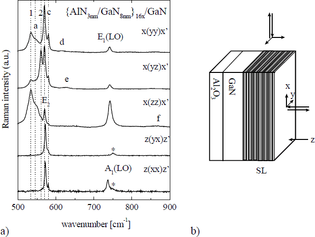
Fig. 1a shows the µ-Raman spectra in five different backscattering configurations. The spectra reveal the A 1(TO), E 1(TO) (labeled by “1”, and “2”, respectively), and E 2, A 1(LO), and E 1(LO) phonon modes of the 1-µm-thick GaN layer which supports the SL.

Figure 1. a) Room-temperature µ-Raman spectra recorded in different backscattering configurations from the AlN-GaN-SL sample (sapphire modes are marked by asterisks). b) Sample setup and directions used for the Porto notations.
The phonon frequencies are summarized in Table I. For convenience, we follow the same notation as used by Gleize et al., and label the additional Raman features within Fig. 1a. at 549, 580, 616, 630, and 860 cm−1 by a, c, d, e, and f, respectively [Reference Gleize, Demangeot, Frandon, Renucci, Widmann and Daudin2]. By changing the position of the Raman beam focus from the sapphire interface toward the sample surface we observed that all of these features are due to the SL. The most prominent line is c at 580 cm−1, which obeys the symmetry behavior of an E 2 mode. Its frequency is close to that of the thick GaN layer. A very similar line was observed by Gleize et al. at 587 cm−1, and was identified as the GaN-sublayer E 2 mode. We also assign c to E 2 of the SL GaN-sublayers. The Raman signal a could belong to a transverse mode with A 1 symmetry. No clear assignment was done in Ref. [Reference Gleize, Demangeot, Frandon, Renucci, Widmann and Daudin2]. A possible origin for this mode might be the A 1(TO) phonon of the AlN-sublattice, but further proof is necessary at this point. Note that we miss the feature labeled b in Ref. [Reference Gleize, Demangeot, Frandon, Renucci, Widmann and Daudin2]. This line was assigned as the SL GaN-sublayer E 1(TO) frequency. As will be discussed below, according to our SL E 2 mode observation at 580 cm−1, the SL E 1(TO) mode should appear ∼570 cm−1, and could therefore be subsumed into the strong E 2 Raman feature of the thick GaN layer at 570 cm−1. The feature labeled d (616 cm−1) was observed at 620 cm−1 in Ref. [Reference Gleize, Demangeot, Frandon, Renucci, Widmann and Daudin2]. It was suggested that this mode may belong to interface excitations. The Raman signal e at 630 cm−1 in Fig. 1a is identified from the IRSE data analysis as the E 1(TO) phonon of the AlN-sublattice (see below). This mode (e) was observed at 635 cm−1 in Ref. [Reference Gleize, Demangeot, Frandon, Renucci, Widmann and Daudin2], but not assigned to a particular sample constituent. The broad and weak structure labeled f is due to a longitudinal mode with E 1 symmetry. Assignment for this mode from the Raman spectra alone is difficult. However, the IRSE analysis proves that this mode belongs to the high-frequency coupled LO-plasmon-phonon (LPP+) mode of the SL GaN-sublayers. The corresponding LPP+ mode with A1 symmetry is not observed because of the strong damping of this axial mode due to the vertical confinement of the carriers to the GaN-sublayers (see discussion below).

Figure 2. IRSE data (symbols: experiment; solid lines: best fit) at 57° ( ) and 72° (![]() ) angle-of-incidence Φ from the AlN-GaN-SL sample. b) Sample setup for the ellipsometric measurement, and definition of Ψ and Δ. rp and rs are the complex reflection coefficients for parallel (p) and senkrecht (s) polarized light.
) angle-of-incidence Φ from the AlN-GaN-SL sample. b) Sample setup for the ellipsometric measurement, and definition of Ψ and Δ. rp and rs are the complex reflection coefficients for parallel (p) and senkrecht (s) polarized light.
Fig. 2a presents the IRSE data together with the best-fit model calculation. As discussed somewhere else in detail ([Reference Schubert, Kasic, Tiwald, Off, Kuhn and Scholz5,Reference Kasic, Schubert, Einfeldt and Hommel6,Reference Schubert, Tiwald and Herzinger9]) for wurtzite III-nitride films on c-plane sapphire, the IRSE data provide less sensitivity to transverse modes with A 1 symmetry. A 1(LO) and E 1 (TO) modes can be identified immediately from resonance structures within the spectra (see Fig. 2a). The E 1(LO) modes follow from lineshape analysis of the IRSE data. The best-fit parameters, and those which were not varied during the regression analysis (values in square brackets), are given in Table I. The E 1(TO) and A 1(LO) frequencies of the “thick” GaN layer are marked within Fig. 2a. The best-fit for the corresponding E 1(LO) frequency resulted in 742 cm−1. These results agree excellently with those obtained from the µ-Raman spectra, and compare well with the known α-GaN modes [Reference Orton1]. The IRSE data are not sensitive to the IR-inactive E 2 modes. Hence, the resonance at 570 cm−1 (b in Fig. 2a) can be immediately identified as the SL GaN-sublayer E 1(TO) mode. Furthermore, the feature labeled e in Fig. 1a proves now as a TO resonance (e in Fig. 2a). It turns out from the IRSE lineshape model calculations that this resonance belongs to the SL AlN-sublayer system. We therefore assign e to the E 1(TO) mode of the AlN-sublayers. The small dip at 875 cm−1 (g) is further assigned to the A 1(LO) mode of the SL AlN-sublayer system. The weak features at 658 cm−1 (e’) and 880 cm−1 (f’) are identified as the E 1(TO) and A 1(LO) modes of the AlN buffer layer, respectively. Gleize et al. [Reference Gleize, Demangeot, Frandon, Renucci, Widmann and Daudin2] used the observed shift of the SL GaN phonon modes to calculate the average biaxial stress σ xx and strain ∊ xx within the SL structure. The elastic coefficients Cij and phonon deformation potential constants (a λ, b λ) for α-GaN were taken from Refs. [Reference Polian, Grimsditch and Grzegory3,Reference Davydov, Averkiev, Goncharuk, Nelson, Nikitina, Polkovnikov, Smirnov, Jacobson and Semchinova4]. Here we find that the GaN-sublayers are subject to an average compressive stress of σ xx ∼ - 4.3 GPa if we consider the shift of ∼ 11 cm−1 for the E 1(TO) mode. This is consistent with the shift of the E 2 mode (∼ 12 cm−1, see Table I). The GaN-sublayer A 1(TO) mode should then appear at ∼ 537 cm−1. The IRSE data are not sensitive to this mode. Unfortunately, we could not find clear evidence of this mode within our µ-Raman spectra. It might be submerged by the stronger A 1(TO) mode of the thick GaN layer. (Note that the total thickness of the SL is only 176 nm.) If elastic deformation of the SL is assumed, the average strain for the GaN layers can be calculated using the Cij’s. We obtain here ∊xx ∼ − 0.9%, which compares well to the in-plane strain (- 0.65%) when both GaN and AlN-sublayers adopt a common in-plane lattice constant, and if we consider the thickness and the relaxed lattice constants [Reference Orton1] for both constituents. This result suggests that the SL adopts a different in-plane lattice constant than the thick GaN “buffer” layer. We note that Gleize et al., who investigated a SL with average Al concentration of 48%, observed a higher strain (-1.3%). This value was also slightly larger than that if a common in-plane lattice constant (-1.1%) is assumed. This might be due to uncertainty of the Cij ’s known so far.
Table I: Phonon mode frequencies of the GaN-AlN-SL in cm−1. Values in square brackets were not varied during the IRSE analysis.

a Raman
b IRSE
c not detectable
d tentative mode assignment
e unstrained GaN, from V. Yu. Davydov et al., J. Appl. Phys. 82, 5097 (1997)
As a unique feature of the IRSE technique, the ellipsometry parameters are sensitive to free-carrier affected changes within the dielectric functions of thin films. In this work we observe that the SL GaN-sublayers contain free carriers. In particular, we obtain from the best-fit regression analysis that both LO A 1 and E 1 modes are coupled to plasmon excitations, and that the “zero’s” of the GaN-sublayer dielectric functions are shifted to higher frequencies [Reference Schubert, Kasic, Tiwald, Off, Kuhn and Scholz5,Reference Tiwald, Woollam, Zollner, Christiansen, Gregory, Wetteroth, Wilson and Powell7]. To quantify carrier concentration and mobility values, the effective mass parameter has to be known. We assume that the carriers within the GaN-sublayer system are free electrons, which may originate from the AlN sublayer system, i.e., from interface and defect induced donor states. Similar carrier effects were observed in unintentionally-doped Al x Ga1− x N layers [Reference Schubert, Kasic, Tiwald, Off, Kuhn and Scholz5]. We further assume an isotropic effective mass, and choose a value of m*/me = 0.22. [Reference Orton1] As a result, we obtain a carrier concentration of ne ∼ 5 1018 cm−3, and a strongly anisotropic carrier mobility. The lateral (electric field polarization E⊥c) mobility µ⊥ ∼ 400 cm2/Vs exceeds the vertical mobility (µ|| ∼ 24 cm2/Vs) by more than one order of magnitude. Note that for “thick” films we observe that in general µ|| ≥ µ⊥ due to the columnar Al x Ga1− x N film growth [Reference Orton1,Reference Schubert, Kasic, Tiwald, Off, Kuhn and Scholz5,Reference Kasic, Schubert, Einfeldt and Hommel6]. In Ref. [Reference Schubert, Kasic, Tiwald, Off, Kuhn and Scholz5] we obtained an isotropic mobility of ∼ 100 cm2/Vs for a 535 nm thick Al0.28Ga0.72N film. The SL result suggests that the free carriers are limited in their mobility perpendicular to the SL interfaces. This may find a simple explanation because of the lateral carrier confinement by the AlN-sublayers. The anisotropic mobility further explains why the LPP+ mode with A 1 symmetry cannot be seen whereas that with E 1 symmetry can be observed within the µ-Raman spectra. It is well known that strong damping of LPP modes hinders their observation by Raman spectroscopy [Reference Kozawa, Kachi, Kano, Taya, Hashimoto, Koide and Manabe10].
To summarize, we investigated a GaN-AlN SL structure by IRSE and polarized µ-Raman scattering. We assigned SL phonon modes by combining results from both techniques. The shift of the GaN sublayer phonon modes allowed us to calculate the average biaxial strain within the SL. The so obtained strain value agrees well with the strain if a common SL in-plane lattice constant is assumed. This study shows strong anisotropic optical carrier effects within the GaN-sublayers. The carriers have very high mobility values for movement parallel to the SL interfaces, and are almost confined for movement parallel to the SL growth direction.
Acknowledgements
Research is supported in part by DFG contract Rh 28-3/1, and in part by NSF contract DMI-9901510.