


Introduction
Rare earth doped semiconductors have been studies for more than a decade because of the possibility to develop compact and efficient electroluminescence devices.Reference Bell 1 , Reference Ennen, Kaufmann, Pomrenke, Schneider, Windschif and Axmann 2 , Reference Pomrenke, Klein and Langer 3 , Reference Coffa, Polman and Schwartz 4 Trivalent Erbium ions (Er3+) are of special interest because they exhibit an atomic-like transition at 1540nm, which corresponds to the low-loss window of silica-based optical fibers. Electroluminescence devices based on Er doped Si and GaAs were reported, however, their efficiency was too low for practical applications.Reference Pomrenke, Klein and Langer 3 , Reference Coffa, Polman and Schwartz 4 An important step forward in the field of Er doped semiconductors was the observation that the room-temperature Er3+ photoluminescence (PL) intensity strongly depends on the bandgap of the host materials. It was found that for larger bandgap energy, there is less detrimental temperature quenching of Er3+ PL occurring.Reference Favennec, Haridon, Salvi, Moutonnet and Le Guillou 5 , Reference Neuhalfen and Wessels 6 Therefore, doping Er3+ ions into wide gap semiconductors is a promising approach to overcome the thermal quenching of Er3+ PL. Consequently, current research efforts focus on studying Er3+ doped into wide bandgap semiconductors such as SiC and GaN.Reference Choyke, Devaty, Clemen, Yoganathan, Pensl and Hässler 7 , Reference Zavada and Zhang 8 First results on the observation of 1.54 μm photoluminescence from Er implanted GaN and AlN were reported by Wilson et al.Reference Wilson, Schwartz, Abernathy, Pearton, Newman, Rubin, Fu and Zavada 9 Subsequently, other research groups reported results of photoluminescence, cathodoluminescence, and electroluminescence (EL) studies of Er implanted GaN. Reference Qui, Leksono, Pankove, Torvik, Feuerstein and Namavar 10 , Reference Silkowski, Yeo, Hengehold, Goldenberg and Pomrenke 11 , Reference Kim, Rhee, Turnbull, Reuter, Li, Coleman and Bishop 12 , Reference Thaik, Hömmerich, Schwartz, Wilson and Zavada 13 The goal for practical device applications is to incorporate Er3+ ions during epitaxial growth. Doping during growth has several advantages over ion implantation including the absence of implantation damage, unlimited layer thickness, and a more homogenous doping profile. In-situ Er doping of AlN using metalorganic molecular beam expitaxy (MOMBE) was first reported by MacKenzie et al. in 1996.Reference MacKenzie, Abernathy, Pearton, Hömmerich, Wu, Schwartz, Wilson and Zavada 14 This work was followed by the first demonstration of in-situ Er doping of GaN.Reference MacKenzie, Abernathy, Pearton, Hömmerich, Wu, Schwartz, Wilson and Zavada 15 Recently, Hansen et al. reported results of in-situ doped GaN: Er prepared by hydride vapor phase growth.Reference Hansen, Zhang, Perkins, Safvi, Zhang, Bray and Kuech 16 Visible PL and EL from GaN: Er grown by molecular beam epitaxy have been reported.Reference Steckl and Birkhahn 17 , Reference Steckl, Garter, Birkhahn and Scofield 18 Even though encouraging strong Er3+ PL results were obtained, initial infrared electroluminescence studies of GaN: Er have shown rather poor efficiencies.Reference Torvik, Feuerstein, Qui, Pankove and Namavar 19 , Reference Shen, Pamulapati, Mackenzie, Ren, Abernathy and Zavada 20 In order to optimize the material preparation for developing more efficient 1.54 μm devices, it is crucial to understand the incorporation and excitation mechanisms of Er3+ ions in III-Nitrides. More specifically, it will be important to identify the Er3+ sites that are excited efficiently through electrical injection of electron-hole pairs and to optimize their concentration in the GaN host.Reference Kim, Rhee, Turnbull, Reuter, Li, Coleman and Bishop 12 In this paper we present new spectroscopic results focusing on the 1.54 μm PL from MOMBE grown Er doped GaN. Results of temperature dependent PL intensity, lifetime, and excitation studies will be shown and discussed for samples with varying oxygen and carbon content. In addition, we will also report some initial results on visible luminescence studies.
Experimental Procedures
The Er doped GaN films were grown by MOMBE in an INTEVAC Gas Source Gen II on In-mounted (100) Si or (0001) Sapphire substrates. The GaN films were preceded by a low temperature AlN buffer (Tg=425 °C). A 0.2 μm undoped GaN spacer was deposited prior to the growth of GaN: Er. Triethylgallium (TEGa), Dimethylethylamine alane (DMEAA), and thermally-evaporated 8N Ga metal provided the group III fluxes. A shuttered effusion oven with 4N Er was used for solid source doping. Reactive nitrogen species were provided by a SVT radio frequency plasma source. Due to the incorporation of carbon and oxygen from residual ether in TEGa, the C and O background observed in TEGa derived GaN were ∼1021cm−3 and ∼1020 cm−3, respectively, as determined by SIMS measurements. GaN grown using thermally-evaporated 8N pure Ga as the group III source had oxygen and carbon backgrounds of less than 1019 cm−3.Reference MacKenzie, Abernathy, Pearton, Hömmerich, Seo, Wilson and Zavada 21
PL measurements were performed using either the broad-band visible (457-514nm) or uv (333.6-363.8nm) outputs of an argon-ion laser for excitation. The luminescence spectra were recorded using a 1-m monochromator equipped with a liquid-nitrogen cooled Ge detector. Visible PL studies employed a thermo-electric cooled photomultiplier tube. The signal was processed using lock-in technique. The samples were cooled on the cold-finger of a two-stage closed-cycle refrigerator. High temperature PL studies were carried out using a homemade heating element, which had a temperature accuracy of ±5°C. Luminescence lifetime data were taken with a fast response Ge detector and averaged using a digitizing oscilloscope. PLE studies were carried out using an argon pumped dye laser or and a Nd: YAG/Optical Parametric Oscillator system.
Results and Discussion
a) Er3+ PL intensity and spectra
Figure 1 shows the room-temperature, infrared PL spectra of Er doped GaN on Al2O3 prepared by MOMBE. No significant spectral differences were observed for Er doped GaN on Sapphire or Si substrates. For comparison, the Er3+ PL spectra of AlN: Er (MOMBE) and Er implanted GaN are also shown in figure 1.Reference Wilson, Schwartz, Abernathy, Pearton, Newman, Rubin, Fu and Zavada 9 , Reference MacKenzie, Abernathy, Pearton, Hömmerich, Wu, Schwartz, Wilson and Zavada 14 All samples were excited with the 363-366.8nm UV output of an Argon-Ion laser. UV excitation was chosen to simulate carrier-mediated Er3+ excitation as in GaN: Er electroluminescence devices. All samples showed characteristic Er3+ PL centered at 1.54 μm, which can be assigned to the intra-4f Er3+ transition Reference Coffa, Polman and Schwartz 4 I13/2--->Reference Coffa, Polman and Schwartz 4 I15/2. The Er3+ PL spectra from in-situ Er doped GaN and AlN are very similar. They exhibit nearly featureless spectra (25-35nm @FWHM) suggesting a homogenous distribution of Er sites as typically observed from Er doped glasses.Reference Miniscalco 22 , Reference Ainslie 23 Er peaks located at 1.517 μm, 1.540 μm, 1.548 μm, and 1.555 μm are either due to Stark splittings and/or multiple Er sites. The overall spectral width of the Er3+ PL from Er implanted GaN was significantly larger (100nm@FWHM) than that observed from Er doped GaN and AlN. Moreover, Er implanted GaN exhibits a more sharply structured Er3+ PL than the in-situ Er doped III-Nitride samples. Based on previously published data 9,10,11,12,13, the more complex and broad Er3+ PL seems to be characteristic for Er implanted GaN samples and is due to a combination of different Er sites and Stark splittings of Er ions in low symmetry sites. For example, Kim et al. identified up to 4 Er sites in Er implanted GaN grown by MOCVD.Reference Kim, Rhee, Turnbull, Reuter, Li, Coleman and Bishop 12 The authors demonstrated that it was possible to selectively excite these four sites by three different below-gap absorption processes and through direct intra-4f excitation. Important for future device development was the observation that only a small fraction of incorporated Er3+ ions are excitable through carrier-mediated processes.Reference Rhee, Kim, Li, Coleman and Bishop 24 Time-resolved PL studies of in-situ Er doped AlN (MOMBE) have indicated the existence of at least two different classes of Er3+ sites with distinct lifetime and excitation schemes.Reference Wu, Hömmerich, MacKenzie, Abernathy, Pearton, Schwartz, Wilson and Zavada 25 These results underline that it is crucial to identify the incorporation and excitation mechanism of Er3+ in different sites in order to optimize the material preparation for device applications.
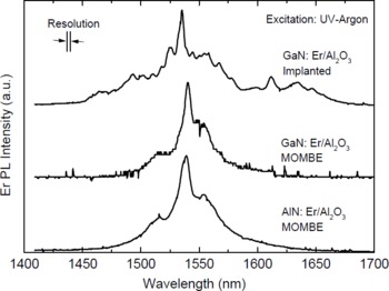
Figure 1: Room-temperature Er3+ PL spectra of Er implanted GaN and in-situ Er doped GaN and AlN.
Figure 2 depicts a comparison of the absolute Er3+ PL intensities of GaN: Er (MOMBE) for below and above-gap excitation at room-temperature. Under below-gap excitation, GaN: Er (TEGa) with high oxygen and carbon background ([O]∼1020cm−3, [C]∼1021cm−3) showed an Er3+ PL peak intensity two orders of magnitude larger than GaN: Er (Ga) with low O and C backgrounds (<1019cm−3). It is interesting to note that also GaN: Er/Si showed strong 1.54μm PL at room temperature, which makes this material attractive for integration with Si based optoelectronics.21 Drastic improvements of the absolute Er3+ PL intensity have been observed for Er and oxygen codoped Si and GaAs. The enhanced 1.54μm PL was attributed to an increased concentration of optically active Er3+ ions and a more efficient Er3+ PL excitation.26,27,28,29,30 Our results for below-gap Er3+ excitation in GaN suggest that the incorporation of O and C introduces beneficial mid-gap states that provide efficient energy transfer pathways for Er3+ in GaN. Support for this idea was obtained from photoluminescence excitation (PLE) studies shown in figure 3. In PLE the effectiveness of stimulating 1.54 μm Er3+ PL is measured as a function of excitation wavelength. The PLE spectra of GaN: Er/Si (TEGa) reveal that the incorporation of high O and C backgrounds leads to a broad PLE band extending over the entire visible region (∼400-800 nm). The GaN: Er (Ga) sample with low C and O content did not show this broad PLE band, but direct intra-4f Er transitions (see e.g. ∼525nm). Therefore, the visible output from an Argon-Ion laser leads to a significantly more efficient excitation of Er3+ in GaN:Er/Si (TEGa) than in GaN: Er/Si (Ga).
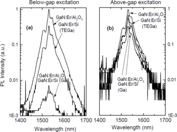
Figure 2: Comparison of Er3+ PL intensity from Er doped GaN (MOMBE) for a) below-gap and (b) above-gap excitation (300K).
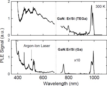
Figure 3: PLE of GaN: Er/Si samples with varying oxygen and carbon content. The incorporation of high oxygen and carbon backgrounds (upper graph) leads to a broad Er3+ excitation band covering the entire visible region.
Under above-gap excitation (figure 2b) all GaN: Er (MOMBE) samples showed a greatly reduced Er3+ PL intensity relative to below-gap excitation, independent of carbon and oxygen concentration. A similar PL reduction was reported for Er implanted GaN.31 It is somewhat surprising that under above-gap excitation the Er3+ PL intensities of samples with high oxygen and carbon backgrounds is only roughly twice as strong as the Er3+ PL observed from low O and C contents. These observations suggest that either only a fraction of optically active Er3+ ions are excited and/or the excitation efficiency is reduced under above-excitation. Moreover, it also indicates that high oxygen and carbon concentrations do not necessary lead to an enhanced luminescence for carrier-mediated Er3+ excitation. More work is necessary to address this issue in more detail.
b) Er PL quenching and lifetime
Figure 4 shows the integrated Er3+ PL intensity of Er doped GaN samples for the temperature range from 15-500K. The Er3+ PL was excited either with the broad-band visible (Fig. 4a) or uv (Fig. 4b) outputs of an Argon ion laser corresponding to below and above-gap Er3+ excitation. Under below-gap excitation a significantly different Er3+ PL quenching behavior was observed for samples with varying O and C contents (see Figure 4a). As was previously observed for Er and oxygen codoped Si and GaAs, GaN: Er samples with high O and C concentrations showed a significantly reduced Er3+ PL quenching compared to samples with low C and O backgrounds.26,27,28,29,30 Between 15K and room-temperature samples with high O and C backgrounds showed Er3+ PL quenching of only ∼20%, whereas the 1.54μm luminescence from low O and C concentration samples decreased by ∼90% over the same temperature range. At higher temperatures also the O and C rich samples showed an enhanced Er3+ PL quenching and the luminescence decreased to roughly 10% of their low temperature value at 500K. Under above-gap excitation the situation was different. As shown in Fig. 4(b) hardly any difference in Er3+ PL quenching behavior was observed for samples with varying oxygen/carbon content. As mentioned above, the oxygen and carbon concentration does not greatly effect the carrier-mediated Er3+ excitation. Up to room temperature the Er3+ PL decreased for all four samples by less than 50% relative to its low temperature value. When heating the samples above room temperature, we observed a steady decrease of the Er3+ PL with increasing temperature. At 550 K, the Er3+ PL from all samples had decreased by nearly 90% of its low temperature value.
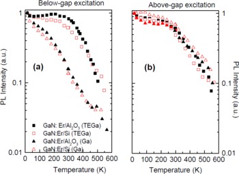
Figure 4: Temperature dependence of the integrated PL intensity from in-situ Er doped GaN for above and below gap excitation.
To gain more insight in the observed Er3+ PL quenching, we performed initial luminescence lifetime studies on the two oxygen and carbon rich samples, GaN: Er/Si (TEGa) and GaN:Er/Sapphire (TEGa). These samples showed the strongest Er3+ PL signal, which allowed us to carry out lifetime studies for the entire range 15-500 K. It was observed that the Er3+ PL decay curves were non-exponential which provides further support for the existence of a wide distribution of Er3+ sites. To describe the luminescence decay an average lifetime <τ> was used:

where I(t) is the luminescence decay curve and t is the time.32,33 The low temperature lifetime of both samples was found to be ∼130μs and decreased to ∼100μs at room temperature. At 500K the lifetime had shortened to ∼50μs. These lifetimes are significantly shorter than previously reported lifetimes for Er implanted GaN, which were in the order of 1-2ms.10,16 It is possible that the short lifetimes are due to a higher oscillator strength of Er3+ transitions in MOMBE grown samples compared to Er implanted GaN. In order to confirm this explanation direct absorption measurements of intra-4 Er transitions are necessary. It is also conceivable that the Er3+ lifetimes are shortened due intra-4f non-radiative decay or cooperative processes such as upconversion or energy migration.34 Power dependent lifetime studies, however, did not show any change in lifetime with increasing excitation density suggesting that the later processes are not dominant in GaN:Er.
It is instructive to compare the temperature dependence of PL intensity and lifetime as shown in figure 5. In the following discussion it is assumed that the Er3+ PL intensity is proportional to the number (or concentration) of excited Er ion (NEr*) and the radiative decay rate (wrad). Under steady state condition and low pump power intensities the Er3+ PL signal can be written as:
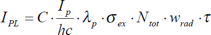
where C is a constant, Ip is the pump intensity, λp is the pump wavelength, σex is the excitation cross-section defined as the product of pump efficiency and absorption cross-section, Ntot is the total Er concentration, wrad is the radiative decay rate, and τ is the luminescence lifetime. Under the assumption that the radiative decay rate and total Er concentrations are temperature independent, the Er3+ PL quenching at higher temperatures can be explained by either the onset of nonradiative deexcitation processes reducing the Er3+ lifetime and/or by a decrease of the excitation efficiency.
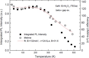
Figure 5: Comparison of the temperature dependence of Er3+ intergrated PL and lifetime for in-situ Er doped GaN.
The comparison of the temperature dependent Er3+ PL intensity and lifetime enables one to separate the above mentioned Er3+ PL quenching mechanism. As can be inferred from figure 5, the Er3+ lifetime follows the change in integrated PL intensity very closely up to room temperature. This means that between 15 and 300K the small decrease in Er3+ PL intensity is due to nonradiative decay. Above room-temperature the lifetime changes less than the integrated Er3+ PL intensity. This suggests that Er3+ PL quenching occurring above room temperature is not only due nonradiative deexcitation, but also due to a reduction in excitation efficiency. Nearly the same Er3+ PL intensity and lifetime behavior was observed for GaN:Er/Si (not shown). Similar to other Er doped semiconductor systems, we assume that the excited Er ion can decay either through emission of a 1.54 μm photon or through non-radiative energy transfer processes to the host (also referred to as “backtransfer” 28,35). It is further assumed that internal Er3+ quantum efficiency does not change with temperature. The change in lifetime is then described by a thermally activated nonradiative decay process, which is controlled by Boltzmann’s law:

where τrad is the radiative lifetime, E is the thermal activation or threshold energy for non-radiative decay, and B is a constant. Fitting equation 3 to the lifetime data shown in figure 5 gives the following parameter values: τrad= 124.6μs, B=31.6, and an activation energy E=132meV. The fit result suggests the existence of a defect-related level close to Er3+, which acts as a particular effective channel for nonradiative energy transfer between Er3+ and the host. The deexcitation of Er ions through some mid-gap level has been discussed before for Er doped Si and GaAs. In the backtransfer model as proposed by Takahei et al.28, the existence of an Er-related level provides the possibility of energy backtransfer where excited Er ions transfer an excited carrier back to the defect level followed by a thermalization into the conduction band. This model for the deactivation of excited Er3+ ions may also be relevant for GaN:Er, however, no experimental evidence for an Er-related defect level has yet been reported. A more detailed comparison of the Er3+ lifetimes of GaN: Er samples with varying oxygen and carbon content is in progress and promises to provide deeper insight in the Er excitation and deexcitation mechanisms.
c) visible PL from GaN: Er
Very recently green luminescence was observed from GaN: Er grown by solid source molecular beam epitaxy under above-gap excitation.36 Narrow lines centered at 537nm and 558nm were identified to be due to the intra-4f Er transitions 2H11/2→4I15/2 and 4S3/2→4I15/2. Subsequently the same authors reported green electroluminescence from Er doped GaN Schottky barrier diodes.37 In figure 6 we show the visible PL spectra of GaN: Er/Sapphire prepared by MOMBE. We observed no green emission lines from any of the investigated samples under below (488nm) or above-gap (325nm) excitation. Interestingly, however, for below-gap excitation we observed a broad red luminescence band, which showed sharp structure at around 665 nm and 690 nm. This emission was not found for the GaN: Er/Si samples. Preliminary studies indicated that the peaks at 665 nm and 690 nm had lifetimes in the millisecond range. The peak at 665 nm is assigned to the 4F9/2→4I15/2 transition of Er3+ ions, whereas the origin of the 690 nm peak is not yet know. The data suggest that the 690 nm line is a pure electronic transition (no-phonon line) accompanied by a vibronic sideband at around 720 nm. A more detailed study is currently being undertaken to identify the origin of the red luminescence from GaN:Er/Sapphire.
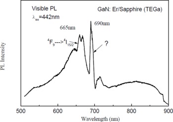
Figure 6: Visible PL spectrum of GaN: Er/Sapphire for below-gap excitation at room-temperature.
Summary
We presented new results on the 1.54 μm luminescence properties of GaN: Er grown by MOMBE. It was observed that high oxygen and carbon concentrations (∼1020 cm−3) enhance the 1.54μm Er3+ PL intensity and reduce the Er3+ PL quenching under below-gap excitation. Moreover, PLE studies revealed that oxygen/carbon introduces a broad below-gap PLE band, which provides an efficient pathway for Er3+ excitation. A direct comparison of the temperature dependence of Er3+ PL intensity and lifetime suggests that both nonradiative decay and a decrease in excitation efficiency reduce the Er3+ PL. Under above-gap excitation the absolute Er3+ PL intensity from all samples was greatly reduced and only a weak PL dependence on the oxygen and carbon concentration was observed. The weak above-gap Er3+ PL suggests that the efficiency of electroluminescence devices (forward biased LED’s) based on currently available materials will be rather low. More materials engineering will be necessary to optimize the 1.54μm Er3+ PL from GaN: Er. Initial results of visible luminescence studies were also presented. It was found that only under below-gap excitation GaN:Er on sapphire emits red luminescence peaking at 665 and 690 nm. The 665 nm line was assigned to an intra-4f Er3+ transition, whereas the origin of the 690 nm line is not yet known. More detailed studies on the luminescence properties of GaN: Er are in progress in will be presented in a forthcoming paper.
Acknowledgments
We would like to thank George Ofori-Boudu and Jakeithia Preajan for the help with some PL experiments. The authors from Hampton University acknowledge financial support by NASA through Grant NCC-1-251 and the Army Research Office through Grants DAAH04-96-1-0089 and DAAG55-98-1-0112. The work at the University of Florida was supported by ARO grant DAAH04-96-1-0089.


