Introduction
Hydride Vapor Phase Epitaxy (HVPE) is a promising technique to grow thick GaN materials. These thick layers can be used in device applications as well as a substrate for subsequent low-defect GaN growth by Metal-organic Vapor Phase Epitaxy (MOVPE) [Reference Detchprohm, Hiramatsu, Amano and Akasaki1,Reference Molnar, Nichols, Maki, Brown and Melngailis2]. Due to the large lattice mismatch, the initial nucleation and growth of GaN on sapphire substrates determines the material properties of the subsequent epitaxial layer. In MOVPE, low temperature GaN or AlN buffer layers have been used to improve this initial nucleation for the subsequent high temperature GaN growth [Reference Nakamura3,Reference Akasaki and Amano4]. In the case of the HVPE process, low temperature buffer layers exhibit poor crystalline quality and lead to the deposition of polycrystalline material at high growth temperatures [Reference Monlar, Gotz, Romano and Johnson5]. The initial nucleation behavior on sapphire, however, can be improved by the inclusion of a ZnO intermediate or buffer layer [Reference Detchprohm, Hiramatsu, Amano and Akasaki1,Reference Molnar, Nichols, Maki, Brown and Melngailis2,Reference Monlar, Gotz, Romano and Johnson5,Reference Ueda, Huang, Spruytte, Lee, Yuri, Itoh, Baba and Harris6]. Based plane ZnO could provide a better lattice match between GaN and sapphire. In many cases, the ZnO buffer layer has been reported not to survive the initial heating and pre-growth treatment and is not reported to be present in the final epitaxial multi-layer structure [Reference Monlar, Gotz, Romano and Johnson5]. Attempts to deposit highest quality ZnO buffer layer to avoid its dissociation from sapphire surface do not lead to further improvements in material quality but rather exhibit poorer properties in the subsequent GaN layer. In this case, some ZnO has been noted at the interface between the high temperature GaN and the sapphire [Reference Ueda, Huang, Spruytte, Lee, Yuri, Itoh, Baba and Harris6]
The mechanism underlying the impact of the ZnO buffer layer on the initial stages of HVPE of GaN material is unknown, particularly in the absence of ZnO in the final structure [Reference Nakamura3,Reference Monlar, Gotz, Romano and Johnson5,Reference Ueda, Huang, Spruytte, Lee, Yuri, Itoh, Baba and Harris6]. ZnO can reactively diffuse into Al2O3 forming a spinel of ZnAl2O4 at high tempaeratures [Reference Keller, Agrawal and Mckinstry7-Reference Branson9]. In previous studies, reactions between ZnO and Al2O3 powders, were limited in the absence of oxygen [Reference Branson9]. In this case, the gas phase transport of ZnO and its stability is affected by the oxygen activity. There is little data on the interdiffusion between epitaxial ZnO and sapphire. ZnAl2O4 surface layer, if present at the growth front, could improve nucleation by lowering the surface energy and could provide an improved lattice match. In this paper, we have studied the formation, annealing and structure of ZnO epitaxial layers on sapphire used to promote nucleation and improve the subsequent GaN growth. In particular, the structure and composition of the ZnO-sapphire interface after high temperature annealing was investigated by atomic force microscopy (AFM), reflection high energy electron diffraction (RHEED), x-ray photoelectron spectroscopy (XPS), and x-ray diffraction (XRD) measurements.
Experiment Detail
ZnO buffer layers were initially deposited on sapphire surface by RF diode sputtering. Prior to ZnO deposition, the bare sapphire wafer was degreased with acetone and methanol followed by etching in a 3:1 sulfuric:phosphoric acid solution at 100°C and a final deionized water rinse. The wafer is then loaded into a RF diode sputtering system employing deposition conditions similar to those reported by Molnar et al [Reference Molnar, Nichols, Maki, Brown and Melngailis2]. ZnO thickness varied from 20 nm to 200 nm depending on the deposition time. RHEED measurements show this as-deposited ZnO film has a high degree of structural orientation. The FWHM of the XRD (002) rocking curves of these films was about 1.3 degrees. Prior to loading in the HVPE reactor, the ZnO coated wafer was again ultrasonically cleaned in acetone and methanol.
GaN was grown on these wafers in a vertical HVPE reactor. The interior structure of the reactor for gas distribution is similar to that of the horizontal system previously reported [Reference Perkins, Horton, Bandic, McGill and Kuech10,Reference Zhang and Kuech11]. In the present system, an additional region called a backflow tube was added which allowed the sample to be heated to the growth temperature under a N2 flow. After loading into the reactor, the ZnO-coated wafer was preheated to the growth temperature in the backflow tube for 10 mins under a flowing N2 environment and then introduced to the flowing growth stream containing the GaCl and NH3 to initiate growth. The flow rate of HCl to Ga source controlled the growth rate over a range of 0.5 to 4 μm/min in this work.
Results and discussion
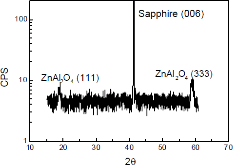
ZnO buffer layer will reactively dissociate under the HVPE pre-growth annealing conditions, leaving a specular surface since it is thermodynamically unstable within an oxygen-free ambient. For buffer layer greater than 20 nm, PL and XRD studies reveal a residual film remains on sapphire surface despite an anneal time sufficient to dissociate this ZnO layer. The thickness of this residual layer depends on the initial ZnO thickness and annealing time. The chemical composition of the specular surface was initially examined by XPS. Prior to the XPS measurement, these samples receiving only the standard pre-growth conditions were dipped into an HCl solution to insure removal of any residual ZnO layer, if present. ZnO is readily etched in HCl. XPS measurements confirm the formation of a thin residual Zn-containing layer on the sapphire surface which is not ZnO. As a contrast, removal of the ZnO layer from sapphire surface prior to the pre-growth annealing results in no detectable Zn signal from the sapphire surface by XPS. These XPS results are shown in Fig.1, for both heat-treated under normal pre-growth conditions, spectrum (a) was obtained from the sample which has the ZnO layer removed prior to annealing and spectrum (b) from a sample etched in HCl after annealing. This figure indicates that some surface Zn remains as a result of a surface reaction that has occurred during pre-growth anneal, not during ZnO deposition process. Spectrum b is very similar to that obtained from ZnAl2O4 formed by annealing mixed ZnO and Al2O3 powder at high temperatures [Reference Strohmeier12], suggesting a thin ZnAl2O4 layer formed during annealing. XRD measurements on this sample were not sufficiently sensitive to detect such a thin layer. In order to confirm the presence of a surface ZnAl2O3 layer by XRD, we annealed a thick ZnO layer on sapphire in air for 30 hrs. The XRD spectrum obtained from this sample shown in Fig.2, contains the (006) sapphire peak, as well as the (111) and (333) diffraction peaks of ZnAl2O4. ZnAl2O4 is a cubic spinel, and the presence of the (111) and (333) peaks indicates a degree of epitaxial alignment in this reactive diffusion couple. This welloriented surface layer will have the (111) texture desired for the subsequent GaN growth.

Fig.1 XPS spectra of Zn-derived sapphire surface after heat-treated under normal pre-growth conditions, (a) removing ZnO layer prior to annealing, and (b) removing ZnO layer after annealing.

Fig.2 spectrum of Zn-derived sapphire surface annealing at air ambience and for 30 hrs.
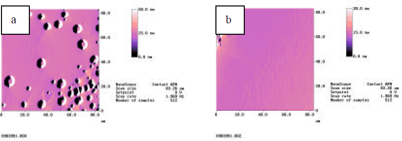
The surface reaction and compound formation modifies the sapphire surface morphology. Fig.3 is the AFM micrograph of the samples used to obtain the spectrum of Fig.1. The surface of sample a has no obvious morphological modification due to the pre-growth anneal and is similar to the bare sapphire surface after annealing in a N2 ambient (not shown here). The surface of sample b is characterized by high density of small islands on the wafer surface. It is this ZnO-derived surface that promotes the enhanced initial nucleation and improved material quality in the subsequent GaN growth.

Fig.3 AFM micrograph of Zn-derived sapphire surface, (a) removing ZnO prior to annealing, (b) removing ZnO after annealing
The surface reaction and compound formation modifies the sapphire surface morphology. Fig.3 is the AFM micrograph of the samples used to obtain the spectrum of Fig.1. The surface of sample a has no obvious morphological modification due to the pre-growth anneal and is similar to the bare sapphire surface after annealing in a N2 ambient (not shown here). The surface of sample b is characterized by high density of small islands on the wafer surface. It is this ZnO-derived surface that promotes the enhanced initial nucleation and improved material quality in the subsequent GaN growth.
GaN growth on the bare sapphire, often leads to a rough surface with inferior material properties. It is often difficult to reproducibly obtain high quality GaN possessing a smooth surface, narrow XRD linewidth, and low carrier concentration. In contrast, the use of ZnO buffer layers, routinely leads to smoother surfaces with few morphology features as well as improved materials properties. Fig.4 contains AFM micrographs of GaN surfaces grown on (a) bare sapphire and (b) an initial 20 nm ZnO buffer layer. The surface pit density is very high for GaN material grown on bare sapphire, which is often associated with the nucleation during initial stages of growth. A surface with the growth features related with step flow growth mode characterize the GaN layer grown on the ZnO buffer layer. XRD measurements on the GaN layers with an 8 μm in thickness possess a (002) rocking curve lindwidth as 400 to 500 arcsec, compared with the GaN layers of a similar thickness grown on bare sapphire normally a linwidth of 700 arcsec or more.

Fig.4 AFM micrograph of GaN material surface morphology (a) on bare sapphire, (b) on 20 nm ZnO buffer layer
Room temperature PL spectra of GaN grown on bare sapphire, a 20 nm thick ZnO buffer layer, and a 80 nm thick buffer layer are shown in Fig.5. The PL spectrum of GaN layer on the 20 nm thick ZnO buffer layer has a slightly narrower bandage emission of 4 to 5 nm of FWHM compared to the FWHM of 7-8 nm for layers grown on bare sapphire. The GaN grown on the ZnO buffer layer also exhibits a weak blue band emission, which has been previously related to Zn doping [Reference Detchprohm, Hiramatsu, Amano and Akasaki1,Reference Ueda, Huang, Spruytte, Lee, Yuri, Itoh, Baba and Harris6]. This blue band emission centered at 420 nm increases in intensity in the PL spectrum of GaN material grown on a thick 80 nm buffer layer, also shown in Fig.5.

Fig.5 Room temperature PL spectra of GaN grown on different buffer layers
Growth on thick ZnO buffer layers can lead to delamination of the GaN layer from substrate, however, no such delamination occurs for materials grown on 20 nm buffer layer. Delamination is associated to the presence of a residual ZnO layer atop of the ZnAl2O4 layer which can persist after the pre-growth anneal for ZnO layers 80 nm or more in thickness. This residual ZnO layer is found to degrade the GaN quality, despite the potential to provide a better lattice matched layer. The line width of the GaN bandedge emission is broader than that found from GaN grown on the thin buffer layer (10 nm or more, depending on growth conditions), as found in a previous study [Reference Ueda, Huang, Spruytte, Lee, Yuri, Itoh, Baba and Harris6]. For our specific system and pregrowth anneal the optimum thickness of the ZnO buffer layer is about 20 nm, which is thick enough to form the surface ZnAl2O4 layer but leaves no residual ZnO prior to starting the growth. Finally, the similar yellow band emissions, seen in Fig.5 for all three samples, is believed to be primarilly related to the specific growth conditions used in the high temperature GaN layers. The intensity of YL can be decreased by a factor of one hundred by changing the growth conditions.
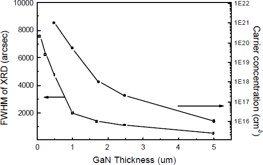
The change in material properties with GaN thickness has also been studied on the optimized ZnO buffer layer as shown in Fig.6. The FWHM of XRD and carrier concentration determining from CV measurements decrease quickly with material thickness. For a 5 μm thick GaN on 20 nm thick ZnO buffer layer, the FWHM of XRD is less than 500 arcsec with a surface carrier concentration as low as 1×10¹⁶/cm3. The GaN surface after 5 μm of growth is smooth with few morphology features. In contrast, GaN grown on bare sapphire exhibits a much slower drop in XRD linewidth and surface carrier concentration with thickness. To achieve a similar materials properties for GaN grown on bare sapphire a layer of 20 μm or more is required in our growth system under similar growth conditions.

Fig. 6 FWHM of XRD (002) and carrier concentration of the GaN materials grown on 20 nm ZnO buffer layer versus material thickness.
Conclusion
ZnO buffer layers provide significant improvements in GaN material quality and system reproducibility by the HVPE method. The formation of a ZnAl2O4 surface layer by reactive diffusion between the ZnO and sapphire during pre-growth annealing process, can improve the initial nucleation and lead to a more rapid improvement in the GaN properties with thickness over layers grown on bare sapphire under similar conditions. The presence of this thin epitaxial ZnAl2O4 layer has been confirmed by XPS and XRD measurements.
Acknowledgements
This work is supported by DARPA-EPRI program on high power GaN devices.