Introduction
The Growth of GaN on sapphire using a low-temperature (LT-) deposited buffer layer [Reference Amano, Sawaki, Akasaki and Toyoda1] followed by the realization of p-type films [Reference Amano, Kito, Hiramatsu and Akasaki2] has lead to the fabrication of bright blue and green light-emitting diodes and violet laser diodes. Nevertheless, the GaN layer still contains high-density threading dislocations on the order of 108 to 1011cm−2 [Reference Lester, Ponce, Craford and Steigerwald3]. Several efforts have been made to reduce the density of threading dislocations, such as epitaxial lateral overgrowth [Reference Usui, Sunakawa, Sakai and Yamaguchi4,Reference Nam, Bremser, Zheleva and Davis5] or pendeo-epitaxy [Reference Zheleva, Smith, Thomson, Gehrke, Linthicum, Rajagopal, Carlson, Ashmawi and Davis6]. In order to achieve much higher performance light emitters and novel devices, reduction of the threading dislocation density together with understanding the growth mechanism on an atomic scale are still one of the most critical and important issues in nitride research.
Very recently, we found a new method of obtaining low-dislocation-density GaN. In the newly developed method, a LT-layer was deposited not only on the sapphire substrate, but also on high-temperature (HT)-grown GaN. Dislocation densities as low as mid-106cm−2 has been achieved by multiple insertion of a LT-layer. This layer deposited between HT-GaN is called the LT-interlayer [Reference Iwaya, Takeuchi, Yamaguchi, Wetzel, Amano and Akasaki7]. High-temperature transmission electron microscopy (TEM) observation was performed to clarify the dynamical process of the LT-interlayer. The as-deposited LT-interlayer is composed of very fine crystallites with a size of about a few nm. First, atomic reconstruction and grain growth occurred in the initial stage of heating. After that, mass transport at the surface occurred. Then the surface became atomically flat. The mass transport leads to a bending of the threading dislocations, thereby achieving low-dislocation-density GaN films on top of the LT-interlayer.
The mass transport at the surface is not limited to the LT-layer, but should also be observed at the surface of HT-GaN. In the case of other III-V materials such as InP, GaAs and GaP, mass transport at the surface is well known and has been reported by several groups [Reference Liau and Walpole8-Reference Ogawa, Akabori, Motohisa and Fukui12]. The essential procedure for the mass transport is the etching of the selected area and annealing in a group-V-source gas containing atmosphere without any supply of group-III source gas. Mass transport at the surface can be applied to fabricate such structures as p-n junctions, quantum dots, buried heterostructure lasers, and gratings for distributed feedback lasers and wafer fusion. Therefore, it is one of the most important key technologies for the fabrication of novel devices. However, there has been no report concerning the mass transport of HT-nitrides. We found that mass transport at the surface of HT-GaN occurs at around the growth temperature [Reference Nitta, Kariya, Kashima, Yamaguchi, Amano and Akasaki13]. We also found that this phenomenon can be applied to grow dislocation-free areas in HT-GaN films on sapphire. In this study, a detailed TEM analysis was performed to clarify the behavior of threading dislocations in the mass-transported region, thereby allowing us to understand the mass transport process on an atomic scale.
Experiment
GaN 7 μm in thickness was grown by metal organic vapor phase epitaxy (MOVPE) on a sapphire (0001) substrate using a LT-AlN buffer layer. Trench stripes were patterned on the surface along the <11-20> direction by reactive ion etching. Several samples of trenches with different depths and widths were prepared. Then, in order to perform mass transport, these samples were annealed at 1100□ in a MOVPE reactor. The temperature was monitored using a thermocouple inserted into the graphite susceptor. During annealing, 0.20 mol/min of ammonia with nitrogen gas was supplied. No group-III alkyl source gas was supplied. After annealing for 12 min, the grooves were almost buried by mass transport processes. To analyze the mass transport process and behavior of dislocations, cross-sectional TEM study was carried out.
Results
Fundamental mechanism of mass transport in shallow trench
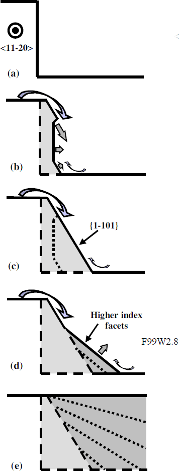
The process of the mass transport of GaN is schematically shown in Fig. 1. Mass transport is generally thought to proceed toward the minimization of total surface energy [Reference Liau and Zeiger14]. Assuming a single mesa step, as shown in Fig. 1(a), at the convex part of the surface, the binding of crystal (Ga-N) is weakened by the higher surface energy. Therefore, GaN is decomposed and free Ga atoms diffuse to the surrounding. On the contrary, at concave part of the surface, Ga atoms are easily reincorporated into the solid and thus growth of GaN occurs. However, the high crystallographic anisotropy, which is characteristic of GaN, modulates the surface shape during mass transport. Therefore, it is hard to form round surface corners composed of higher index facets as observed in the case of InP [Reference Liau and Zeiger14]. {1-101} facets of GaN are energetically much more stable than other facets, except for {0001}, as has already been reported by other groups [Reference Kato, Kitamura, Hiramatsu and Sawaki15,Reference Kitamura, Hiramatsu and Sawaki16]. Thus, once the facets are formed at the upper trench edges, decomposition does not continue there. Therefore, the Ga species are supplied from the outer area of the surface, as shown in Fig. 1(b). Other stable facets such as {1-100} are formed before the {1-101} facet plane is completely formed, as shown in Fig. 1(c). Then, once {1-101} facets from both upper edges are connected to each other or reach the bottom of the groove, higher index facets are formed and the trench is gradually buried, as shown in Figs. 1(d) through 1(e).

Fig. 1 Scheme of process of mass transport in GaN in shallow trench.
Mass transport in deep trench and mechanism of void formation
Fig. 2 schematically shows the process of mass transport into a deep trench. If the trench is deeper than the crossing point, a void is formed under the V-groove groove, as shown in Fig. 2(c). In the case of a deep trench, {1-101} facets from each upper edge are formed prior to other facet. Therefore, the connecting point is geometrically determined by the angle between (0001) and {1-101} facets. We should bear in mind that there is a small offset for {1-101} facets to form in both sides, because there is also growth toward [1-100] the direction. Once {1-101} facets are connected, forming a void under the V-groove, no more Ga species are supplied, resulting in void formation.

Fig. 2 Scheme of process of mass transport in GaN in deep trench. If the trench is deeper than the crossing point, a void is formed.
Behavior of threading dislocations
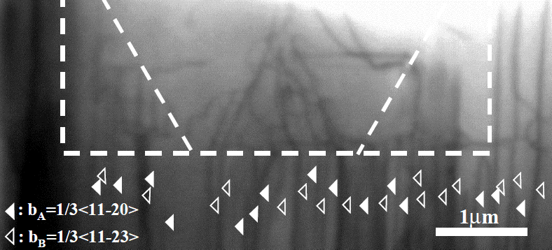
Fig. 3 shows the bright-field cross-sectional TEM image of the 4.5 μ;m wide trench after mass transport. This figure indicates several important aspects of mass transport. Dislocation-free regions were obtained in the upper areas of the left-half center and the right-half center of the trench. Threading dislocations reaching the bottom of these areas are bent. Therefore, they should not propagate to these regions. In the initial stage of mass transport, threading dislocations near the side wall continue to propagate vertically, and then bend horizontally when they reach the {1-101} facet surfaces which were formed during mass transport. The effect of this particular plane has already been reported by Sakai et al. [Reference Sakai, Sunakawa and Usui17]. However, during burying, some of these dislocations propagate toward the surface again. On the contrary, the direction of propagation of the threading dislocations that reach the bottom of the central part of the trench is changed by the higher index facet plane. Then, these dislocations merge to the center of the trench. In this case, crystallographic anisotropy of the higher index facet plane is not so high as in the case of {1-101}. Therefore, the dislocations bend toward the free surface in order that the energy should be minimum. From dark-field TEM images (not shown here) most of these dislocations are divided into two types with a Burger’s vector of either bA=1/3<11-20> (type-A) or bB=1/3<11-23> (type-B). Each type-A and –B dislocation is indicated by a solid or open arrowhead, respectively. Fig. 4 schematically shows the behavior of each dislocation. A type-A dislocation is simply bent horizontally in the <11-20> or <1-100> direction, as shown in Fig. 4(a). On the contrary, a type-B dislocation propagates vertically until it reaches {1-101} facets. At the {1-101} facets the dislocation is bent horizontally in the <1-100> direction. However, when higher index facet growth appears, the dislocation propagates along the growth direction, as shown in Fig. 4(b). Both type-A and -B dislocations retain the Burger’s vector direction even after bending.

Fig. 3 Cross-sectional TEM image of shallow trench after mass transport.

Fig. 4 Schematic images of behavior of dislocation which has (a) bA=1/3<11-20> or (b) bB=1/3<11-23>.
Conclution
Processes of mass transport for the cases of shallow and deep trenches involving the mechanism of void formation were clarified. The cross-sectional TEM study indicated that threading dislocations which have a Burger’s vector of either bA=1/3<11-20> or bB=1/3<11-23> were bent by the mass transport process. It was found that the behavior of threading dislocations is strongly affected by the mass transport process as well as high crystallographic anisotropy of the surface energy of facets particular to GaN. Mass transport is found to be very effective for the growth of low dislocation density GaN on sapphire. It is also useful for growing highly pure GaN, because this method does not require any masks, which sometimes act as an impurity source.
Acknowledgements
This work was partly supported by the Japan Society for the Promotion of Science (JSPS) Research for the Future Program in the Area of Atomic Scale Surface and Interface Dynamics under the project "Dynamic Process and Control of the Buffer Layer at the Interface in a Highly-Mismatched System", and the Ministry of Education, Science, Sports and Culture of Japan (contract no. 11450131).