


1. Introduction
Three growth techniques are simultaneously investigated in our laboratory for the attainment of electronic quality GaN layers. Hydride Vapor Phase Epitaxy (HVPE), where growth is obtained via the reaction of NH3 with Ga chlorides (Tg ~ 1030 °C) have been used for a long time, and the first physical investigation of GaN material properties were performed on HVPE grown crystals Reference Dingle, Sell, Stokowski and Ilegems[1] Reference Monemar[2]. HVPE allows large growth rates (30-80 μm/h) and can be used for pseudo-homoepitaxy purposes. Metal-Organic Vapor Phase Epitaxy (MOVPE) uses the reaction of Ga metalorganics (TrimethylGallium in our case) with nitrogen precursors, mainly NH3(Tg = 1000-1100 °C) and to date has allowed the attainment of high quality nitride based structures, recently illustrated by the realisation of pulsed mode blue laser diodes operating at room temperature Reference Nakamura, Senoh, Nagahama, Iwasa, Yamada, Matsushita, Kiyoku and Sugimoto[3]. Gas source molecular beam epitaxy (GSMBE) is a new exploratory technique. Expected advantages should come from the low growth temperatures used (~800 °C) and low gas consumption. Also, the in situ characterization tools of MBE are invaluable Reference Grandjean, Massies and Leroux[4]. In this work an optical characterization of GaN layers grown on (0001) Al2O3 by the three above techniques is presented. Temperature dependent photoluminescence (PL) and reflectivity experiments were performed. Due to the importance of strain effects, mainly of thermoelastic origin, in a strongly mismatched system as GaN/Al2O3 Reference Gil, Briot and Aulombard[5], these two techniques are complementary. Reflectivity, providing intrinsic energy levels, is indeed essential in the interpretation of PL transitions, mainly of extrinsic origin. Well resolved reflectivity spectra, allowing the identification of the three (A, B and C) excitonic levels of GaN, can be obtained, whatever the growth technique Reference Leroux, Beaumont, Grandjean, Golivet, Gibart, Massies, Leymarie, Vasson and Vasson[6]. The results will be mainly concerned with nominally undoped samples, but also with Mg doped MOVPE-grown ones.
2. Results and discussion
Figure 1 displays the luminescence spectra at 9 K of three undoped GaN samples grown by HVPE, GSMBE and MOVPE, from top to bottom. The thicknesses are 100, 0.8 and 3 μm respectively. The residual n-type doping is evaluated to ~1018 cm−3 for HVPE and GSMBE samples and below 1017 cm−3 for the MOVPE one. The three spectra are dominated by band edge excitonic transitions involving free exciton A, donor bound exciton (I2, 6 meV lower in energy than A) and acceptor bound exciton (I1, 10 meV lower than A) recombinations Reference Dingle, Sell, Stokowski and Ilegems[1] Reference Monemar[2] Reference Leroux, Beaumont, Grandjean, Golivet, Gibart, Massies, Leymarie, Vasson and Vasson[6]. The energy of all these lines varies (whithin 10 meV in our samples) with the biaxial strain level, and reflectivity spectra are indispensable for the identification of these PL transitions, by providing the energy of the free exciton states. In the 3.27 eV range are observed donor-acceptor pairs (D0A0) recombination involving the usual residual donors and acceptors of GaN Reference Strite and Morkoç[7]. Their depths are evaluated to 35±5 and 220±5 meV respectively Reference Leroux, Beaumont, Grandjean, Golivet, Gibart, Massies, Leymarie, Vasson and Vasson[6], from an analysis of their excitation intensity dependence Reference Zacks and Halperin[8]. This is in agreement with earlier determinations Reference Strite and Morkoç[7]. Inspection of figure 1 shows that the ratio of band edge to acceptor related transitions increases when going from HVPE to GSMBE to MOVPE grown samples, at least at present. This is in agreement with the highest purity measured by Hall effect in MOVPE samples. Of course, in GaN, impurities does not necessarily mean atom impurity.

Figure 1. Luminescence spectra (log scale) at 9 K of nominally undoped GaN/Al2O3 samples grown by HVPE, GSMBE and MOVPE, from top to bottom.
2.1 MOVPE-grown GaN
The lower spectrum shown in figure 1 is typical of high purity MOVPE grown GaN. Residual acceptor related luminescence is hardly observed in such samples. Besides band edge excitons, dominated by I2, low intensity lines (labelled D1D′1) can be observed in the 3.38-3.9 eV range. They are attributed to phonon replica of free exciton luminescence or to free hole-deep donor transitions (or to deeply bound excitons) in which the hole is weakly bound Reference Leroux, Beaumont, Grandjean, Golivet, Gibart, Massies, Leymarie, Vasson and Vasson[6]. Due to the low residual n-type doping level, efficient p-type doping using Mg can be achieved, and will be discussed in the following. Figures 2a and 2b display the evolution of near edge luminescence of MOVPE-grown GaN with increasing Mg doping. Also shown is a nonintentionnally doped sample for comparison (the spectrum is equivalent to that shown in figure 1). In a weakly Mg doped sample (G103, still n-type), one notes in addition to the residual (D0A0) band and its LO phonon train a new band, ~40 meV lower in energy (labelled D0Mg0). With increasing Mg doping (samples G112, G269), this new band dominates the spectra, and simultaneously shifts towards lower energies (figure 2a). Eventually, at larger doping level, the spectrum becomes dominated by a broad 'blue band' peaking at 2.8-2.9 eV, depending on samples, as shown in figure 2b. This behaviour has already been reported Reference Gotz, Johnson, Walker, Bour and Street[9] Reference Beaumont, Vaille, Lorenzini, Gibart, Boufaden and el Jani[10] Reference Smith, Chen, Lin, Jiang, Salvador, Sverdlov, Botchkarev, Morkoc and Goldenberg[11] and can be due to a deepening of acceptor levels, of donor levels, or both. Figure 3 displays the excitation intensity dependence of the PL peak of the D0Mg0 band. In sample G103, the variation of the peak energy can be accounted (solid lines) assuming a 30-40 meV donor and acceptors of ~220 meV (A0) and ~265±10 meV. This last value is ascribed to Mg0 acceptors, and is in agreement with refs Reference Orton[12] Reference Eckey, Holst, Maxim, Heitz, Hoffmann, Broser, Meyer, Wetzel, Mokhov and Baranov[13]. As such, we may tentatively assign the series of sharp lines near 3650 Å in the spectrum of sample G103 to close D0Mg0 pairs of type I. The D0Mg0 transitions are replicated by 90±5 meV phonons with a Huang-Rhys factor S of 1±0.2. With increasing Mg doping level, the shift with excitation intensity of the 3.2 eV donor-acceptor pair band increases (figure 3). This rather suggests the apparition of deep compensating donors. Eventually, deep centers, or band tailing, occur, corresponding to the 'blue band' . Note that such a behaviour is qualitatively similar to that encountered in the luminescence of p-type (nitrogen) doped ZnSe, other wide gap semiconductor. Occurrence of deep compensating donor levels rather than deep acceptor states is in agreement with the fact that the Hall depth of Mg acceptors is 150-170 meV whatever the doping level Reference Gotz, Johnson, Walker, Bour and Street[9].
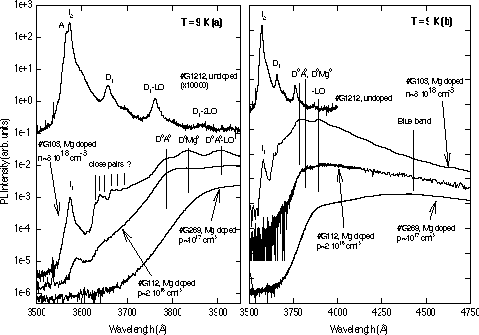
Figure 2. Luminescence spectra at 9 K of undoped and Mg doped MOVPE-grown GaN, with increasing Mg doping levels. (a): near edge transitions. (b): on an expanded energy range.
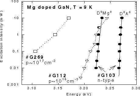
Figure 3. Excitation intensity dependence of the peak energies of donor-acceptor pair bands in Mg doped GaN for various doping levels. Solid lines are a fit according to reference Reference Zacks and Halperin[8]. Dotted lines are guides to the eyes.
2.2 HVPE-grown GaN
Figure 4 displays the PL and reflectivity spectra of an undoped 100 μm thick HVPE-grown GaN sample. The reflectivity spectrum, with an A exciton energy of 3.472 eV, indicates that the layer is fully relaxed Reference Gil, Briot and Aulombard[5]. The various PL transitions observed have been described above. What we shall discuss is the broad pedestal observed on the PL spectrum, extending on the high energy side up to the layer's band gap. On figure 4 is also given the luminescence spectrum recorded from the substrate side. It consists of a broad band, with a high energy cutoff at ~ 3.6 eV. To understand such a line shape, we show in figure 5 the PL and reflectivity spectra of an n+ (n = 4 1019 cm−3) HVPE grown sample. The high residual doping level is presumably due to the fact that this sample was grown using ammonia which was not purified by molecular sieves in line. The PL spectrum is also broad, with a large low energy tail, and a rather sharp high energy cutoff well above the pure GaN's band gap. Such spectrum ressemble those of type II or type III GaN, in the terminology of reference Reference Dingle, Sell, Stokowski and Ilegems[1]. We interpret it as in the case of n+ GaAs, i.e. as due to indirect transitions between acceptor like tail states and electrons up to the Fermi level Reference Levanyuk and Osipov[14]. In particular, the half-intensity high energy cutoff E1/2agrees with the energy of recombinations between tail-localized holes and Fermi edge electrons Eg+EF−ET, as expected Reference Levanyuk and Osipov[14] (figure 4). We then ascribe the broad pedestal observed on the PL spectrum of high purity HVPE-grown GaN (figure 5) to partially reabsorbed PL from an interfacial n+ layer.

Figure 4. Luminescence and reflectivity spectra at 9 K of a 100 μm thick undoped HVPE grown GaN sample. PL spectra are given recorded from the surface and substrate faces.
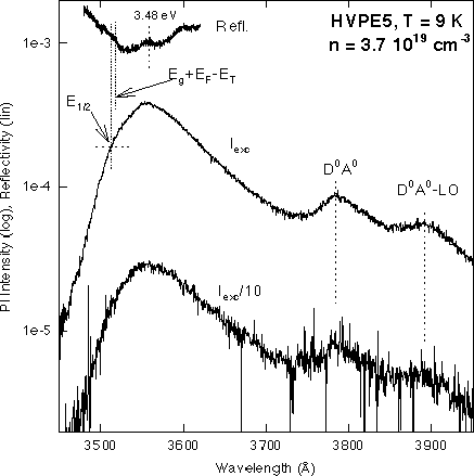
Figure 5. Luminescence and reflectivity spectra (9 K) of an n+ HVPE grown GaN layer.
2.3 GSMBE-grown GaN
As mentionned previously, the high vacuum conditions of MBE allow the use of in situ characterization tools. Combining in situ Reflection High Energy Electron Diffraction experiments and ex situ PL, an optimized sapphire nitridation procedure has been defined Reference Grandjean, Massies and Leroux[4]. The spectrum of a 8000 Å thick GSMBE grown layer is displayed on figure 1. Besides already discussed transitions I2 and D0A0, to be noted is a band at 3.404 eV and labelled D2. On another hand, the PL spectra of layers that are only 600 Å thick are dominated by a band peaking at 3.425±0.005 eV Reference Grandjean, Massies and Leroux[4], and attributed to free hole-oxygen donor recombinations, according to reference Reference Chung and Gershenzon[15]. We then tentatively ascribe the D2 band in the spectrum shown in figure 1 to transitions involving O impurities, the source of oxygen being possibly diffusion from the sapphire substrate.
3. Conclusions
GaN/Al2O3 layers grown using three different techniques, MOVPE, HVPE and GSMBE have been characterized using luminescence and reflectivity experiments. Well resolved reflectivity spectra can be obtained whatever the growth technique, allowing strain effects to be taken into account in the interpretation of the PL spectra. Samples displaying excellent optical quality, with luminescence dominated by sharp band edge exciton lines, have been grown. MOVPE allows at the present stage to grow the highest purity samples. This allows efficient p-type doping by magnesium. An optical depth of 260-270 meV for Mg acceptors is deduced from our characterization.
Acknowledgments
The help of P.Lorenzini, S.Laügt, G.Nataf and C.Golivet was invaluable. We thank B.Gil (CNRS, Montpellier) for numerous and fruitful advices. Discussions with G.W.Orton (Nottingham University) are also acknowledged. This work is supported in part by an European Community ESPRIT LTR Contract LAQUANI 20968.


