


Introduction
Combining ferroelectric oxide materials with III-nitride wide band gap semiconductors presents a special interest for a number of areas including high-speed image processing and high power microwave devices and circuits. For example, high-speed, high-density arrays of spatial light modulators based on ferroelectric (electro-optic) films can be controlled by GaN based field effect transistors (FETs). The advantages of AlGaN/GaN FETs compared to their Si-H based counterparts are high operation voltages and transparency in visible and near UV range. Stratified high-ε oxide/III-nitride structures can be also used as an advanced voltage variable capacitors (varactor) with wide tuning range for microwave applications. Fundamental properties of III-N semiconductors and their heterostructures, such as high thermal conductivity, break-down voltage and saturation velocity, chemical and mechanical stability, high density 2DEG in heterostructures make them superior to Si and GaAs for high power applications. Gallium nitride also possesses a distinctive advantage over arsenide or phosphide semiconductors with its higher thermal stability. For example, thermal annealing in nitrogen at 850°C indicated no deterioration of photoluminescent and electrical properties [Reference Davydov, Anderson and Moustakas1]. This allows fabrication compatibility and use of higher processing temperatures and more optimal growth conditions for oxide films on GaN.
In this work we report on growth and characterization of electric and electro-optic properties of high-quality oxide films of (Pb,La)(Ti, Zr)O3 (PLZT) and (Ba,Sr)TiO3 (BST) families on GaN/c-sapphire structures.
Experimental
Silicon doped n-type GaN layers, which have been used as a substrate for PLZT deposition, were grown by metalorganic chemical vapor deposition on c-oriented sapphire. The GaN layers, 5 µm thick, were fully relaxed, as evidenced by high resolution X-ray diffraction measurements with electron concentration and Hall mobility of 2·10 cm18 and ∼360 cm·V−1sec−1·respectively. The solution of lead, zirconium, barium, strontium and lanthanum carboxylates, and titanium isopropoxide in water-methanol mixture was used to grow PLZT and BST films. The temperature of the ferroelectric films’ growth was kept between 650-700°C to avoid decomposition of GaN and to reduce the chemical interaction between GaN and PLZT in the interface layer. Thickness of the ferroelectric films was in 0.3-5 µm range. Deposition was performed using standard dip-coating technique. Details of the deposition procedure are described elsewhere [Reference Fuflyigin, Li, Wang, Jiang, Liu, Zhao, Norris, Yip and Tendeloo2].
XRD spectra were recorded on “Rigaku” diffractometer using CuKα radiation. Films thickness was measured using profilometry, i.e. “Dektak”. Ferroelectric measurements were taken using standard Sawyer-Tower scheme. A HP4140A picoampermeter was used for I-V characterization of the grown films.
Results and Discussion.
Ferroelectric properties of PLZT films on GaN.
Oxide films deposited on GaN with or without ITO layer showed good adhesion to the substrate, and passed the “scotch tape” test. X-ray diffraction (XRD) measurement indicated that both PLZT and BST films were single phase and polycrystalline without predominant texture. We deposited 20-40 nm thick layer of ITO on GaN in order to obtain a highly (110)-textured ferroelectric oxide films (Figure 1). Details of this approach are given in [Reference Fuflyigin, Osinsky and Wang3]. Orientation of the ferroelectric films appears to be one of the most important factor affecting their electro-optical properties. In PLZT phase with composition 8/65/35 (“rhombohedral” phase), polar axis is parallel to [111] direction. In (110)-oriented PLZT films the [111] direction lies in the substrate plane and is, therefore, perpendicular to the incident light beam. In this arrangement, maximum phase retardation between ordinary and extraordinary components of the light beam can be reached, if the material is used in transmission mode. Therefore, the control of the ferroelectric film orientation is very critical if electro-optic applications are implied.
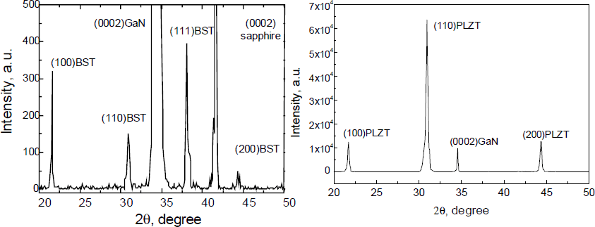
Figure 1. X-ray diffraction patterns of the 0.3 µm thick BST film on GaN/c-sapphire (left) and 3 µm thick PLZT film grown on ITO/GaN/c-sapphire. (right)
As it was shown by AFM study, PLZT films on GaN had a submicron grain size. This is smaller than the wavelengths used in optical communication systems, which are 1300 and 1550 nm. Hence, small optical loss related to the scattering on grain boundaries can be expected.
For characterization of electric properties of PLZT/n+-GaN and PLZT/ITO/ n+-GaN structures, vertical test capacitors were fabricated. Rectangular Au/Ti contact pads with 0.3×0.5 mm2 area were deposited by e-beam evaporation on the top of the oxide films. Highly conductive n+-GaN epilayer served as a bottom electrode to the ferroelectic film. Ohmic contact to the n+-GaN bottom electrode was made using Ti/Al.
PZT and PLZT films exhibited a well-pronounced ferroelectric behavior with remnant polarization Pr in the range of 20-25 µC/cm2 (Figure 2). Ba0.5Sr0.5TiO3 composition which was used in our experiments corresponds to high-ε paraelectric phase. Understandably the ferroelectric hysteresis loop was not observed for BST films grown on GaN/c-sapphire.

Figure 2. Ferroelectric hysteresis loop measured for PLZT film with composition 8/65/35 grown on ITO/GaN/c-sapphire.
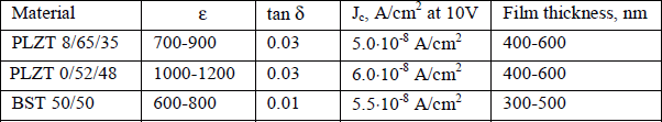
Table I summarizes dielectric properties of the fabricated PLZT and BST films. All these materials possess relatively high dielectric constant. This speaks out for good crystallinity of high-ε layers. It is also worth mentioning that leakage current density measured on the grown films is under 6.0⋅10−8 A/cm2 at 10V. This further proves high quality of the synthesized oxide layers.
Table I. Dielectric properties of the PLZT and BST films deposited on GaN.
Electro-optic properties of PLZT films on GaN.
To characterize the electrooptic properties of the PLZT films on the hexagonal GaN, the method of phase-modulated differential ellipsometry was employed in a reflection mode. Details of this method are described in [Reference Wang, Furman and Haertling4]. The schematic in Figure 3 shows the arrangement of the optical path and electrodes. The phase modulated He-Ne laser beam entered the c-cut sapphire substrate from the side opposite to where GaN and PLZT were grown. The laser beam was transmitted through the substrate, the GaN layer, the thin ITO layer before entered the PLZT layer; upon reflection from the aluminum electrode, the beam again was transmitted through all the layers then collected by the phase sensitive detection system. A slow varying voltage signal was applied to the aluminum electrode and the conductive GaN or ITO/GaN layers. In this arrangement, the field-induced birefringence as a function of the applied field could be recorded. A theoretical model for calculating field-induced birefringence of the stratified structures was employed in processing the measured data.

Figure 3. The structure of the device with ferroelectric/GaN integration and the light path during the characterization of the electrooptic properties of the PLZT layer. The thickness of the GaN layer and that of the PLZT layer are 5 and 3 microns, respectively.
The field-induced birefringence, Δn, of a PLZT layer on an n-GaN/c-sapphire wafer was measured as a function of the applied voltage. The thickness of the PLZT layer was 3 microns. As shown in Figure 4, the PLZT layer was highly electrorefractive. Under electric field strength of approximately 30 V/µm, a field-induced birefringence as high as 0.02 was measured, which was among the highest reported for all solid materials. The large field-induced birefringence was expected from the high dielectric polarization of the films measured under a similar external field. With the increase of the external electric field, a saturation behavior in the field-induced birefringence became obvious. Saturation of this kind is quite common in ferroelectric materials, resulting from the saturation in the material polarization vs. electric field hysteresis curve. Two other characteristics were also noticeable in the electro-optic response curve, i.e., the hysteretic behavior and the asymmetry of the loop. Although the selected PLZT composition normally exhibit ’slim-looped’ electro-optic response, the rather ’fat’ hysteresis loop was not very surprising.

Figure 4. Field-induced birefringence of the PLZT layer in the ferroelectric/GaN integrated structure as a function of the external electric field.
It is well known that the polarization hysteresis loops of ferroelectric thin film materials can be altered severely by the properties of the substrates. In the absence of lattice matching, the difference between the films and their substrates in thermal expansion often create mechanical stress that in turn causes changes in their ferroelectric properties. Judging from the known thermal expansion properties of the materials, the PLZT films should be under a compressive stress. The asymmetry in the polarization hysteresis loop may be a result of several factors including; nonuniform stress distribution in the growth direction, different nature of the top and bottom electrode materials, and formation of the depletion region in semiconductor layers. A similar phenomenon was observed in an ITO/PLZT/Pt structure.
Figure 4. also shows an electro-optic hysteresis loop taken under UV illumination (dashed line). The measurements were taken from the described structure illuminated with UV light from xenon lamp. One can see that with UV illumination the hysterisis loop becomes more symmetric. The reason for it could be photoinduced space charges in the PLZT film or generation of non-equilibrium carriers in the GaN depletion layer. It appeared that photogenerated carriers reduce the width of the depletion region in semiconductor materials, which results in a more symmetric loop. The understanding of this phenomenon is in progress.
Conclusions.
High quality films of PLZT and BST were successfully grown by sol-gel technique on hexagonal conductive n+GaN epitaxial layers. We found that the introduction of a 20-40 nm thick indium tin oxide (ITO) layer between PLZT and GaN results in highly (110)-textured PLZT layer with remnant polarization as large as 20-25 µC/cm2 and strong electrooptic properties. BST films on GaN demonstrated low frequency dielectric constant as high as 800 with very low leakage currents. Field-induced birefringence of 0.02 was measured in Al/PLZT/ITO/GaN vertical capacitor structure. UV illumination from xenon lamp was found to result in a more symmetrical electrooptic hysteresis loop. We relate this to the photoinduced charge in the semiconductors depletion region at negative and positive biases.


