Introduction
With the demonstration and commercialization of III-V nitride edge-emitting laser diodes [Reference Nakamura and Fasol1], the emphasis in the research area is gradually shifting to the fabrication and demonstration of vertical cavity surface emitting laser (VCSEL) structures [Reference Honda, Katsube, Sakaguchi, Koyama and Iga2-Reference Song, Zhou, Diagne, Ozden, Vertikov, Nurmikko, Carter-Coman, Kern, Kish and Krames4]. An important requirement for the operation of such a device is the use of high reflectance mirrors, usually in the form of distributed Bragg reflectors (DBRs). Honda and co-workers [Reference Honda, Katsube, Sakaguchi, Koyama and Iga2] have estimated the threshold current density in a GaN VCSEL structure and concluded that an increase in the peak reflectance of the DBR mirror from 90% to 99% results in more than an order of magnitude reduction in the threshold current density. Another important requirement for the fabrication of nitride VCSEL structures is the large bandwidth of the primary reflectance peak. This is important because the active region of the nitride lasers is based on InGaN heterostructures or multiple quantum wells, whose emission spectra are very sensitive to small variations in growth or process parameters. Specifically, the InGaN alloys were found to undergo both phase separation and ordering [Reference Singh, Doppalapudi, Moustakas and Romano5-Reference Doppalapudi, Basu, Ludwig and Moustakas6].
Two different approaches have recently been proposed for the fabrication of VCSEL structures based on III-V nitrides. In the one approach SiO2/HfO2 dielectric λ/4 stacks were used as top and bottom mirrors and flip-chip mounting techniques and laser-induced separation of the nitride structure from the sapphire substrate were employed to complete the device [Reference Song, Zhou, Diagne, Ozden, Vertikov, Nurmikko, Carter-Coman, Kern, Kish and Krames4]. The alternative approach used DBRs based on 35-pairs of Al0.34Ga0.66N/GaN as the bottom mirror and SiO2/TiO2 as the top mirror [Reference Someya, Tachibana, Lee, Kamiya and Arakawa3]. The second approach has the advantage that the nitride active region of the device can grow epitaxially on the top of the nitride DBRs.
The main difficulty in fabricating nitride DBRs with high reflectivity and large bandwidth is the small index of refraction contrast that can be obtained within the entire AlGaN alloy composition. A number of groups have reported the fabrication of AlGaN/GaN DBRs with peak reflectance in the near-UV to blue-green region of the spectrum [Reference Khan, Kuznia, Hove and Olson7-Reference Fritz and Drummond11]. With the employment of 30−40 quarterwave periods, peak reflectivities at 390 nm of 96% were obtained with a bandwidth of about 14 nm. DBRs based on AlN/GaN quarterwave stacks have the potential for higher peak reflectance and larger bandwidth with approximately half the number of quarterwave periods.
We have previously reported that a 20.5 period DBR had peak reflectance of 95% at 392 nm [Reference Ng, Doppalapudi, Iliopoulos and Moustakas10]. The morphology and the reflectance of the structures were uniform across the 2-inch wafer. However, the simulation of the experimental data using the transmission matrix method required a variation of the thickness of the AlN (GaN) layers by as much as 30% of their nominal value. Thus in order to improve the performance of such DBRs, it is imperative to accurately control the thickness of the individual layers. Such control is more important in nitrides than in similar devices based on GaAs/AlAs because the thicknesses of the quarterwave layers in the nitrides are 400−600 Å while those for the arsenides are approximately 800−1000 Å.
In this paper, we report on the growth and characterization of high reflectivity AlN/GaN DBRs with peak reflectance up to 99% and bandwidth up to 45 nm.
Simulations
Simulations using the transmission matrix method [Reference Macleod12] were performed in order to design the DBR structures. The transmission matrix formulation is given by


where nsubs and nr are the refractive indices of the substrate and the rth layer respectively, dr is the geometrical thickness of the corresponding quarterwave layers and λd is the target wavelength for the peak of the high reflectance band. For the simulation, we have used the thicknesses of the AlN and GaN layers of 53.1 and 46.1 nm respectively while the refractive index values of AlN, GaN (λ= 450 nm) and sapphire used were 2.12, 2.44 and 1.78 respectively. We have assumed constant refractive index values for AlN and sapphire for the wavelength region of interest (λ > 400 nm). However, the dispersion of the GaN refractive index has to be taken into account in the simulation and we have modeled it using the Sellmeir equation [Reference Born and Wolf13].
The optical admittance is given by

and the reflectance is defined by

Figure 1 shows the calculated peak reflectance of an AlN/GaN DBR (λ = 450 nm) with varying number of quarterwave periods. We see that a calculated peak reflectance of 99% or greater can be achieved using 16 or more periods in the DBR.

Figure 1: The calculated peak reflectance of an AlN/GaN DBR (center wavelength = 450 nm) with varying number of periods from 10 to 20.
Experimental Methods
The DBR structures were deposited in a Varian Gen II MBE unit equipped with an ASTeX compact ECR microwave plasma source to activate the molecular nitrogen. The sapphire substrate was first subjected to a plasma nitridation at 150W microwave power at 800°C to convert the Al2O3 surface to AlN [Reference Ng, Doppalapudi, Korakakis, Singh and Moustakas14]. An AlN buffer layer of ∼25 nm was deposited at 750°C. The quarterwave stack was then deposited at a growth rate of 0.35μm/h with the substrate temperature at 750°C. A total of 20.5 – 25.5 periods of AlN/GaN were deposited starting with AlN. Fluxes were calibrated from the growth rates of bulk layers.
The cross-section of thick AlN/GaN bilayers as well as of the DBRs were studied using a JEOL 6010 electron microscope. Thick AlN/GaN bilayers were grown in the growth run preceding the actual growth of the DBR structure to calibrate the growth rates of the two binaries. The reflectance of the DBRs was measured at normal incidence using a Xenon lamp as the light source. The reflected beam was dispersed through a 0.5m grating spectrometer and detected with a photomultiplier tube attached to the exit slit of the spectrometer. The reflectance spectrum of the DBR was normalized to the spectrum taken with a calibrated Al-mirror (Melles-Griot) in place of the sample.
Results and Discussion
The cross-section SEM image of one of the DBR structures is shown in Fig. 2 where the entire 20 periods of the structure can be observed. The lighter layers represent AlN while the darker layers represent GaN. The interface between AlN and sapphire is also shown in the figure.

Figure 2: Cross section scanning electron micrograph of the entire DBR stack. The lighter layers represent AlN and the darker layers represent GaN.
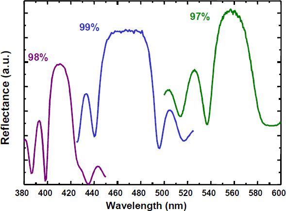
The normalized reflectance spectra of a number of DBR structures with peak reflectance ranging from violet to green wavelength regions are shown in Fig. 3. We have also previously reported a DBR with center wavelength at 392 nm (in the near-UV) with peak reflectance of 95% [Reference Ng, Doppalapudi, Iliopoulos and Moustakas10]. For the samples shown in the figure, the highest peak reflectance of 99% was measured for the sample with a center wavelength of 467 nm and a bandwidth of 45 nm. The peak reflectance region can be tuned to different wavelengths based on the thicknesses of the AlN and GaN quarterwave layers designed.

Figure 3: Reflectance spectra of three AlN/GaN DBRs with peak reflectance of 98%, 99% and 97% at center wavelengths of 410, 467 and 560 nm respectively
In some samples, we have observed a network of cracks on the surface of the sample which we attribute to the tensile stress in the AlN layers. In order to prevent the cracking, we have grown some samples with an asymmetric structure using AlN layers thicker than the GaN layers to increase the mechanical yield strength of the AlN layers. We observed that the cracking has been reduced but we do not have empirical data to ascertain the strain state of the AlN layers at this time. The spectra on the left and right show smaller bandwidths compared to that of the one in the middle. Those two structures are asymmetric DBRs with the AlN layers three times thicker than the GaN layers. For such structures, the simulations show that the peak reflectance and the bandwidth will be reduced compared to the ideal case. To compensate for the reduced reflectance due to the asymmetry, the number of periods of the DBR can be increased. The samples on the left and right side of Fig. 3 have 25.5 and 20.5 periods respectively.
Figure 4 shows the results of the simulation in comparison to the measured reflectance spectrum of the DBR with peak reflectance in the blue wavelength region (shown in Fig. 3). The simulation shows excellent agreement with the experimental reflectance spectrum in terms of the peak reflectance, the bandwidth of the high reflectance region as well as the relative locations of the sidelobes.

Figure 4: Measured and simulated reflectance spectra of the AlN/GaN DBR with center wavelength at 467 nm and peak reflectance of 99%.
Summary
In conclusion, we have designed and fabricated high reflectivity DBRs using AlN/GaN quarterwave stacks. For the best sample, peak reflectance greater than 99% at 467 nm has been achieved using 20.5 periods. This paves the way for the fabrication of optoelectronic devices such as vertical cavity surface-emitting lasers, resonant-cavity light emitting diodes and photodetectors using the III-nitride system.
Acknowledgements
The authors would like to thank Mr. E. Iliopoulos for helpful discussions and Mrs. Anlee Krupp for help with the SEM measurements. This work was partially funded by ONR under grant no. N00014-98-1-0213 (monitored by Dr. C.E.C. Wood).