

1. Introduction
For all structures discussed bellow 6H-SiC and 4H-SiC wafers were used as substrates. All structures except GaN/SiC heterostructures were grown by metal organic chemical vapor epitaxy (MOCVD) Reference Dmitriev, Irvine and Edmond[4]. Hydride vapor phase epitaxy (HVPE) Reference Melnik, Nikitina, Zubrilov, Sitnikova, Musikhin and Dmitriev[5] was employed for GaN/SiC p-n heterojunction fabrication. Usually GaN was deposited on (0001)Si face of the substrate (the p-n junction plane was perpendicular to the c crystal axis). In MOCVD grown structures, Si and Mg were used as donor and acceptor impurities, respectively. Ni, Ti or Pd metals was employed to form ohmic contact top-GaN Reference Vassilevski, Rastegaeva, Babanin, Nikitina and Dmitriev[6] and Al, Ni or Ti/Ni ohmic contacts were formed to n-GaN Reference Vassilevski, Rastegaeva, Babanin, Nikitina and Dmitriev[7]. Mesa structures were formed by reactive ion etching (RIE) Reference Vassilevski, Sizov, Babanin, Melnik and Zubrilov[8].
2. GaN p-n junctions
In this section we will discuss characteristics of GaN p-n homojunctions. The first GaN p-n junction was reported in 1989 Reference Amano, Kito, Hiramatsu and Akasaki[9]. Since, significant progress has been achieved on fabrication of GaN p-n structures Reference Akasaki and Amano[10] Reference Nakamura, Mukai and Senoh[11] Reference Goldenberg, Zook and Ulmer[12] Reference Khan, Chen, Skogman and Kuznia[13] Reference Molnar, Singh and Moustakas[14] Reference Dmitriev, Irvine, Edmond, Carter, Kuznetsov, Zubrilov, Kalinina and Tsvetkov[15] Reference Dmitriev, Irvine, Carter, Kuznetsov and Kalinina[16]. However, published information on the main properties of these junctions(i.e., impurity distribution in the junction, built-in voltage, current flow mechanism, breakdown characteristics) still is very limited. We will describe two types of the junctions fabricated on silicon carbide substrates: (1) linear graded p-n junctions and (2) abrupt p-n junctions. Mesa structure diameter ranged from 100 to 300 μm. The p-n junctions were characterised in terms of capacitance-voltage (C-V) and current-voltage (I-V) characteristics. The position of the p-n junction in the structure was determined by electron beam induced current. The concentration of electrically active uncompensated impurities, [Nd-Na], was measured using C-V characteristic of GaN p-n junction or Shottky barrier.
2.1 Linearly graded GaN p-n junctions
GaN layers of n- and p-type were grown subsequently in the same epitaxial run (Figure 1). A typical thickness for n- and p-layer was ~2 μm and ~0.5 μm, respectively. The concentration Nd - Na in n-layer was ~ 2x1018 cm-3.Na - Ndconcentration in p-GaN layer ranging from 3x10¹⁷ to 1x1018 cm-3. At the surface Na - Nd value was increased up to ~1019 cm-3.

Figure 1. Schematic drawings of the GaN p- n homojunction: 1 - Pd contact to p-GaN, 2 - p-GaN layer, 3 - n-GaN layer, 4- Al contact to n-GaN, 5 - buffer layer, 6 - 6H-SiC substrate.
2.1.1. C-V characteristics
C-V characteristics of the diodes were linear when plotted in V-C-3 coordinates. This indicates that the p-n junctions had a linear impurity distribution. The built-in violate, Vbi, determined by C-V measurements ranged from 2.2 to 2.6 V. The impurity gradient (α) in the p-n junction was determined from C-V data to be from 2x10²² to 2x1023 cm-4 for different samples.
2.1.2. Forward I-V characteristics
The I-V characteristics were measured for current densities from 10−10 to 10 A/cm2in the temperature range from 200 to 600 K. At a forward voltage less than ~2.2 V, the forward current density, J, was an exponential function of applied voltage (Figure 2):

Figure 2. Forward I-V characteristics for linearly graded GaN p- n junction: 1 - 250 K, 2 - 300 K, 3 - 400 K, 4 - 500K, 5 - 600 K.
where Jo is the saturation current density and n is the ideality factor. In the temperature range from 200 to 400 K ideality factor n was dependent on temperature and ranged from 7 to 2.4. It means that in this temperature range current flow mechanism cannot be explained by a classical model for carrier recombination in a space charge region Reference Sze[17]. At temperatures higher than 450 K, n is equal to ~2 and is independent of temperature. In this high temperature region, the saturation current density Jo showed an exponential dependence on temperature(Figure 3):

Figure 3. Saturation current for GaN p- n junction as a function of temperature.
where Jo* is the pre-exponential factor and Ea is an activation energy being close to half of the GaN band gap. Thus, we may conclude that for the temperature range from 450 to 600 K the current flow mechanism in the GaN p-n junctions may be described by the Sah - Noyce -Shockley model for carrier recombination in a space charge region Reference Sah, Noyce and Shockleyin[18]. At high current densities the I-V characteristics were determined by contact resistance of the contact top-GaN.
2.1.3. Reverse I-V characteristics
The reverse I-V characteristics showed abrupt breakdown at voltage ranging from 40 to 150 V. Breakdown voltage, Vb, was determined as the voltage at which an abrupt change in the reverse I-V characteristics occurred (Figure 4). The breakdown had a microplasmic nature. Microplasms were seen by direct observation. At reverse voltages less than breakdown voltage (V <0.9xVb), the leakage current at room temperature was less than 10−6 A (J = 10-2 A/cm2).

Figure 4. Reverse I-V characteristics for linearly graded GaN p- n junction (300 K).
It was found Reference Dmitriev, Irvine, Carter, Kuznetsov and Kalinina[16] that the strength of the electric breakdown field for the GaN p-n junctions ranged from 1.5 to 3 MV/cm. This value is approximately 4 times higher than the maximum breakdown field for a linearly graded GaAs p-n junction at the same impurity gradient.
As was mentioned before, we did not see uniform electric breakdown. This means that the obtained E values do not represent the maximum strength of the electric breakdown field, Em, in GaN, but may be used to estimate a lower limit of Em(Em > E). The exact value of Em for GaN p-n junctions must be measured on p-n structures having uniform breakdown over the entire p-n junction area.
Breakdown voltage increases with temperature. The temperature coefficient of the breakdown voltage was measured to be ~2x10⁻⁴ K-1 for a sample having α = 3x1022 cm-4.
2.2 Abrupt GaN p-n junctions
Another type of GaN p-n structures was grown in two different epitaxial runs. In the first run, p-GaN 1.5μm thick layer having Na-Nd concentration of ~1019 cm-3was grown. Then, in the second run n-n+ GaN structure was deposited. Thickness of the n-layer was 0.7 μm. Thickness of then+-layer was about ~0.1 μm. Surface Nd-Na concentration was ~1019 cm-3. Device structure is shown in Figure 5. Mesa diameter was 100 μm.

Figure 5. Schematic drawings of the abrupt GaN p- n homojunction: 1 - Ti/Ni contact to n-GaN, 2 - n+-GaN layer, 3 - n-GaN layer, 4 - Ti contact to p-GaN, 5 p-GaN layer, 6 - buffer layer, 7 - 6H-SiC substrate.
2.2.1. C-V characteristics
The C-V characteristics of the structures were linear then plotted in V-C-2coordinates indicating that p-n junction was abrupt. The cut-off voltage of the C-V characteristics for different samples ranged from 2.7 to 3.5 V (300 K).
2.2.2. I-V characteristics
In a low current density region (J <1 A/cm2), the forward current density was an exponential function of applied voltage and may be described by equation 1. In the temperature range from 300 to 620K ideality factor n was dependent on temperature and ranged from 2.5 to 1.5. The current flow mechanism is under investigation.
At a higher current density (J > 10A/cm2) the I-V characteristics were determined by resistivity of the p-GaN layer. High resistivity of p- GaN is due to relatively low carrier concentration (p ~ 5x1017 cm-3, 300K), low carrier mobility (μp ~10 cm2V/s), and small thickness of p-GaN layer (~1.5 μm).
The reverse I-V characteristics showed abrupt breakdown at voltage ranged from 40 to 60 V. This value is a few times less than may be expected for breakdown field measured for linear graded p-n junction and Nd-Na concentration in n-GaN layer determined from C-V measurements (Nd - Na ~ 1017cm-3). We believe that in this case the p-n junction breakdown is due to n-region pinch off. To measure the real breakdown field for abrupt GaN p-n junction the base region of the diode should be thicker or Nd-Na concentration higher.
2.3 Electroluminescence of GaN p-n junctions
Electroluminescence (EL) spectra for GaN p-n junctions (Figure 7) usually contained an edge peak at ~365 nm (hν ~3.4 eV), impurity attributed peaks in the range from 410 to 460 nm (2.7 - 3.0 eV), and the so-called "defect" peak at ~550 nm (~2.25 eV). A detailed description of edge peak properties is given in reference Reference Zubrilov, Tsvetkov, Nikolaev, Soloviev and Dmitriev[19]. Depending on growth and doping conditions and on the GaN p-n junction design, each of the peak scan dominate the EL spectrum.

Figure 6. Forward I-V characteristics for GaN abrupt p- n junction: 1 - 290 K, 2 - 336 K, 3 - 410 K, 4 - 500 K, 5 - 623K.

Figure 7. Electroluminescence spectra for a GaN p- n homojunction (300 K, J = 20 A/cm2).
3. AlGaN p-n junctions
Moving towards the shorter wavelength region requires the active region of the emitter to have a wider band gap than that for GaN (EgGaN ~3.4 eV, which corresponds to λ of ~365 nm). Here we describe p-n junctions formed inside AlGaN alloys Reference Dmitriev, Irvine, Carter, Zubrilov and Tsvetkov[20].
AlGaN p-n junctions were grown on 6H-SiC substrates by MOCVD. Band gap diagram of the p-n structure and device structure are schematically shown in Figure 8. First n-GaN layer about ~1.5 μm thick was grown. After that the p-n homojunction or heterojunction was formed between two layers of AlGaN. Then a p+-GaN cap layer ~0.5 μm thick was grown. The maximum AlN concentration in AlGaN layers was ~8 mol.%. Mesa structures diameter was 300 μm. Pd and Al were used as materials for ohmic contacts for p-type and n-type GaN, respectively. Capacitance-voltage characteristics indicated that these junctions were linearly graded. The built-in voltage was Vbi = 4 - 8 V indicating the existence of a compensated region inside the junction.

Figure 8a. Schematic drawing of the AlGaN p- n junction structure: 1 - Pd contact to p-GaN, 2 - p-GaN layer, 3 - p-AlGaN layer, 4 - n-AlGaN layer, 5 - Al contact to n-GaN, 6 - n-GaN layer, 7 -buffer layer, 8 - 6H-SiC substrate.

Figure 8b. Schematic drawing of the aluminium composition profile.
The EL spectra of the structures was measured at room temperature. The edge EL peak which position depends on AlN concentration in the structure was detected. We attribute this peak to carrier recombination in one or both AlGaN layers. The dependence of photon energy for the EL edge peak on AlN concentration in the base AlGaN layer (the layer with the smaller AlN concentration in the case of p-n heterojunctions) is shown in Figure 9. The minimum wavelength of EL peak of ~348 nm (hν ~ 3.56 eV, 300 K) was measured for Al0.08Ga0.92N/Al0.06Ga0.94N heterostructure.

Figure 9. Dependence of the photon energy of the electroluminescence edge peak on AlN concentration in AlGaN (300 K) for AlGaN p- n junction, dashed line is a linear approximation for direct bandgap - composition dependence for AlGaN alloys.
When the thickness of n-AlGaN layer was small (<0.3 μm), the EL peak situated at 365 nm was detected in the spectrum. It was believed that injected carriers may reach the n-GaN layer and peak at 365 nm is attributed to carrier recombination in n-GaN region. For the structure having n-AlGaN layer ~0.5 μm thick, EL spectra did not contain the edge peak at λmax ~365 nm. It was assumed that in this structure, the n-AlGaN layer is much thicker and carrier recombination is taking place in AlGaN.
4. GaN and AlGaN p-i-n structures
Semiconductor p-i-n structures are of scientific and practical interest. P-i-n structures may be used in optoelectronics and high-frequency electronics. Along with them being practical, investigation of p-i-n structures gives us an understanding of the physics of semiconductor materials.
GaN and AlGaN p-i-n structures were grown by MOCVD on 6H-SiC substrates Reference Kuznetsov and Dmitrievin[21]. For n-type layers doped with Si concentration Nd-Na was about ~1x1018cm-3. For p-type layers doped with Mg concentration Na-Nd ranged from 3x10¹⁷ to ~1x1019 cm-3.First ~2 μm thick GaN layer with Nd-Na~1x1018 cm-3 was grown. Then GaN or Al0.08Ga0.92N p-n homojunctions were formed. On the top of the p-n junctions a 0.5 μm thick cap p+GaN layer was grown atop the p-n junction. The structures were grown by the way providing formation of a highly compensated i-region between the n- and p-layers. Mesa structure diameter was 300 μm. Pd and Al were used as ohmic contacts for p+-GaN and n-GaN, respectively. A planar device geometry was used (Figure 10).

Figure 10. Schematic drawings of a GaN p-i-n structure: 1 - Pd contact to p-GaN, 2 - p-GaN layer, 3 - i-region, 4 - Al contact to n-GaN, 5 - n-GaN layer,, 6 - buffer layer, 7 - 6H-SiC substrate.
4.1 C-V characteristics
The C-V characteristics of the GaN and AlGaN p-i-n junctions were linear when plotted in C-2 - V coordinates. Built-in voltage for the GaN p-i-n structures determined by the C-V measurements ranged from 4 to 7 V. This value is larger than that for a normal GaN p-n junctions doped with Si and Mg. The difference due to an i-region located in the structure. The width of the i-region was found from C-V measurements to be about 0.1 μm.
4.2 I-V characteristics
Typical forward current-voltage(I-V) characteristics of GaN p-i-n structures are shown in Figure 11. The I-V characteristics contain power-law regions (I ~ Vb, where b ranged from 1 to 10). At temperatures less than 100 K and forward voltage of about 15 V, s-shape of forward I-V characteristic was observed. Such current behaviour is typical for p-i-n structures. The measured forward I-V characteristics follow the model Reference Ashley and Milnes[22] describing current transport in p-i-n structures with i-regions having deep-level impurities. A single recombination centre is assumed, which, in equilibrium is partially occupied by electrons. Also it is assumed that the capture-cross sections of the recombination centres are different for holes and electrons. The activation energy of these recombination centres was extracted from the temperature dependence of the forward current at fixed voltage. Plots of log(I) - 1/T are linear with a slope corresponding to an ionisation energy of 0.146 eV and of 0.191 eV for the GaN and the AlGaN p-i-n structures, respectively.
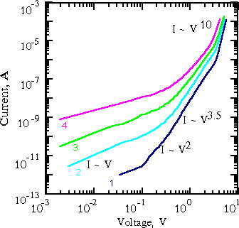
Figure 11. Forward I-V characteristics of a GaN p-i-n junction: 1 - 300 K, 2 - 400 K, 3 - 500 K, 4 - 600 K.
Reverse I-V characteristics of the p-i-n structures showed abrupt breakdown at voltages ranging from 20 to 90 V. The strength of the breakdown electric field was estimated to be ~ 3 MV/cm for GaN and AlGaN structures.
To determine parameters of deep centres in the structures the current-transient mode deep-level transient spectroscopy (i-DLTS) was used Reference Kuznetsov[23]. Presence of hole traps was detected. The values of the ionisation energy for deep level in GaN and Al0.08Ga0.92N p-i-n structures determined by i-DLTS measurements (0.141 eV for GaN and 0.207 eV for AlGaN, respectively) are in good agreement with ionisation energy for Mg acceptor measured using the Hall effect Reference Tanaka, Watanabe, Amano, Kobayashi, Akasaki, Yamazaki and Koike[24].
5. n-GaN/p-SiC heterojunctions
The direct deposition of GaN on SiC provides one the opportunity to create devices based on GaN/SiC heterojunctions. Recently GaN has been successful grown on SiC substrates without buffer layers by HVPE. The deposition technique was described elsewhere Reference Melnik, Nikitina, Zubrilov, Sitnikova, Musikhin and Dmitriev[5]. The thickness of the GaN layers ranged from 0.5 to 2 μm. GaN growth rate was controlled from 0.02 to 0.4 μm/min.
Mesa-structures (150 μm diameter) were formed by RIE (Figure 12). The capacitance-voltage (C-V) characteristics of the GaN/SiC p-n heterojunctions were linear when plotted in C-m-V coordinates, where the coefficient m ranged from 2.5 to 2.7. The cut-off voltage of C-V characteristics was about 2.0 V. This value is close to the built-in potential for n-GaN/p-6H-SiC heterojunction estimated using Anderson's model and found to be ~2.2 V Reference Kuznetsov, Gubenco, Nikolaev, Melnik, Blashenkov, Nikitina and Dmitriev[25].

Figure 12. Schematic drawings of a GaN/SiC p- n structure: 1 - Ti/Ni contact to n-GaN, 2 - n-GaN layer, 3 - p-6H-SiC substrate, 4 - contact to p-SiC.
The structures showed good rectifying characteristics for GaN/SiC p-n heterojunctions (Figure 13). Breakdown voltage ranged from 15 to 100 V. The turn on voltage of forward I-V characteristics was ~2 V which corresponds to built-in potential. It should be note that the value of cut-off voltage determined from C-V measurements is close to the turn on voltage for forward I-V characteristics.

Figure 13. I-V characteristics of a GaN/SiC p- n junction (300 K): vertical scale - 0.5 mA/division, horizontal scale- 2 V/division.


