Introduction
Because GaN is a wide-bandgap semiconductor, it is commonly assumed that large quantities of point defects will be present, because of self-compensation affects. For example, the first GaN, grown some thirty years ago, was strongly n-type, and the natural assumption was that the relevant donors were associated with the N vacancy VN [Reference Maruska and Tietjen1]. Only recently has this idea been shown not to be true, at least for the best, present-day GaN epitaxial layers [Reference Look, Reynolds, Hemsky, Sizelove, Jones and Molnar2]. In fact, accurate first-principles theoretical calculations indeed suggest a low concentration of VN centers in n-type GaN, but a much higher concentration of Ga vacancy VGa defects [Reference Neugebauer and Van de Walle3]. However, the theoretical calculations assume equilibrium growth conditions, which may not be true, especially for the molecular-beam epitaxial (MBE) process. In fact, at the present time, MBE-grown GaN layers contain higher concentrations of donors, acceptors, and traps, than layers grown by metal organic chemical vapor deposition (MOCVD), or hydride vapor phase epitaxy (HVPE). The question is whether those donors, etc., are associated with defects, or impurities, or both. With regard to line defects, i.e., dislocations, the situation is somewhat clearer. It is known that dislocations act as nonradiative recombination centers [Reference Evoy, Craighead, Keller, Mishra and DenBaars4], and affect the performance of GaN-based light emitters [Reference Mukai, Takekawa and Nakamura5]. More recently, it has been shown that they are also strong scattering centers, especially at the typical concentrations found in mismatched GaN/Al2O3 layers [Reference Look and Sizelove6]. Finally, there is evidence from deep-level transient spectroscopy (DLTS) experiments, that dislocations act as traps [Reference Auret, Goodman, Koschnick, Spaeth, Beaumont and Gibart7]. The VN center also is a trap [Reference Fang, Hemsky, Look and Mack8].
Besides point defects and dislocations, there are two-dimensional defects, such as stacking faults, which we will classify as areal defects [Reference Romano, Krusor and Molnar9,Reference Stampfl and Van de Walle10]. Recent theory suggests that stacking faults in GaN are not electrically active [Reference Stampfl and Van de Walle10]; however, it is also known that the heavily-faulted interface region between HVPE GaN and the Al2O3 substrate is strongly n-type [Reference Look and Molnar11], possibly due to donor-like defects, although impurities cannot be ruled out. Thus, point, line, and areal defects all may play important roles in determining the concentrations of donors, acceptors, traps, and recombination centers in GaN.
Line Defects: Dislocations
In GaN layers with high dislocation densities, the mobilities are usually low [Reference Keller, Keller, Wu, Heying, Kapolnek, Speck, Mishra and DenBaars12]. However, until recently, it was not clear whether or not dislocations had a direct or indirect effect on mobility. For example, one of the two layers shown in figure 1 has a much higher mobility than the other, and also a much lower dislocation density [4 × 108 cm−2 vs. 2 × 1010 cm−2, respectively, as measured by transmission electron microscopy (TEM)]. But there are also other differences in the samples, which might be expected to have an even greater effect on the mobilities. To quantify the scattering effects of dislocations, we recently showed that the scattering rate for a line charge, such as a dislocation, is given by the inverse of the following relaxation time [Reference Look and Sizelove6]:
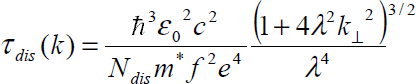
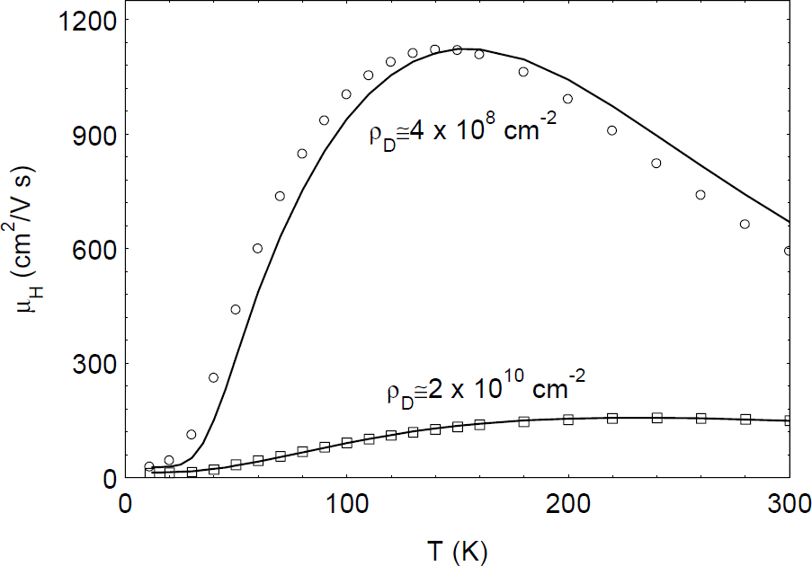
Figure 1. Hall mobility as a function of temperature for two MOCVD GaN samples with different dislocation densities (ρD’s). The solid lines are theoretical fits.
where c is the c-lattice distance (5.185 Å), f/c is the linear charge density, λ is a screening parameter, k⊥ is the wave vector in a direction perpendicular to the c axis, and the other symbols have their usual meanings. Since λ ∝ n1/2, it can be seen that dislocations are strongly screened by free electrons, and thus affect mobility more in the better (lower-n) samples. By adding the scattering rates of other important scattering mechanisms, and solving the Boltzmann transport equation to determine mobility, data sets such as those shown in figure 1 can be fitted, and parameters such as Ndis determined from the best fit [Reference Look and Sizelove6]. The agreement shown in figure 1 is excellent, especially considering that the only fitting parameters, other than Ndis, are the donor concentration ND and energy ED. With an assumption of one negative charge per c-lattice distance (f=1), the fitted dislocation densities are 4.2 × 10⁸ and 2.3 × 1010 cm−2, respectively, in very good agreement with the TEM results. First-principles theory suggests that a likely configuration for the dislocation core in n-type GaN includes vacancies at the Ga sites [Reference Wright and Grossner13]. It is expected that Ga vacancies could hold up to three negative charges per site (f=3); however, a theoretical analysis which includes electron-electron repulsion [Reference Leung, Wright and Stechel14] leads to a value of about one charge per site (f=1), in agreement with the Hall results [Reference Look and Sizelove6]. Note that such dislocations can strongly compensate the layer; e.g., 2 × 10¹⁰ dislocations per cm2 will compensate (2 × 10¹⁰)/(5.185 × 10−8)=4 × 10¹⁷ electrons per cm3, a higher value than that found in some high-quality GaN layers these days. Dislocation densities less than 108 cm−2 will have little effect on the mobility of present-day samples, but may become important again as impurity and defect levels are eventually reduced to the 1015-cm−3 level. It should also be pointed out that, besides being strong scattering centers, there is good evidence that dislocations can also act as recombination centers (RCs) [Reference Evoy, Craighead, Keller, Mishra and DenBaars4] and traps [Reference Auret, Goodman, Koschnick, Spaeth, Beaumont and Gibart7]. With regard to the latter, consider trap C1, shown in the data of figure 2; pulse-filling studies verify that this trap has unusual capture kinetics, more suggestive of a line charge (dislocation) than a point charge. Note that trap and RC effects often begin to show up at far lower defect concentrations than those found to be important for compensation and scattering. Thus, efforts to rid GaN of threading dislocations should be vigorously pursued.
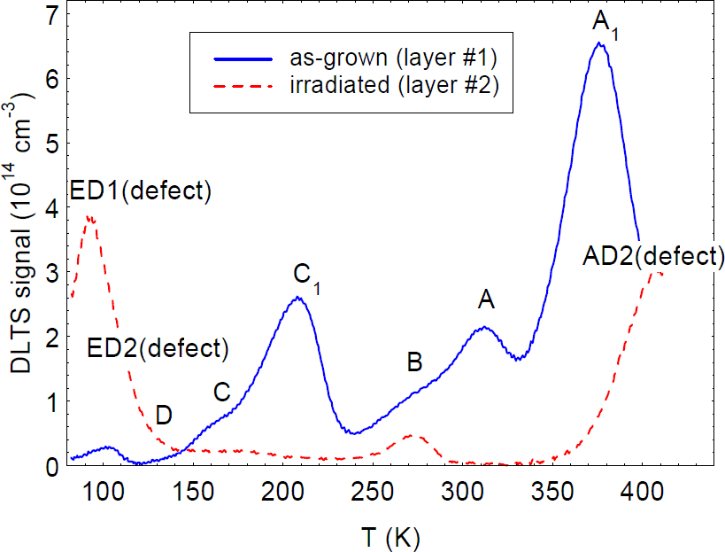
Figure 2. DLTS spectra for an as-grown MBE GaN layer (solid line), and an irradiated MOCVD GaN layer (dashed line).
Areal Defects: Stacking Faults
Type I stacking faults (one violation of the stacking rule) in GaN have a small formation energy (10 meV per unit-cell area), and thus are expected to be abundant [Reference Stampfl and Van de Walle10]. Indeed, they are quite common in GaN, especially near the film/substrate interfaces [Reference Romano, Krusor and Molnar9]. In HVPE-grown GaN, especially, a region of about 2000-Å thickness near the GaN/Al2O3 interface is heavily faulted, and, interestingly, this same region is strongly n-type, often with a sheet density of about 1015 cm−2 or greater [Reference Look and Molnar11]. There is some disagreement in the literature whether or not stacking faults (SFs) should have electronic levels in the band gap; one theoretical calculation finds a level at EV + 0.13 eV [Reference Bandić, McGill and Ikonić15], while another finds no levels at all [Reference Stampfl and Van de Walle10]. Neither of these scenarios can explain the highly degenerate n-type region, so that the origin of these shallow donors remains a mystery. It is possible that other donor-type defects, such as N vacancies, are present along with the SFs, or there may be a high concentration of impurity donors, such as ON. In any case, this interface region has a strong effect on the measured electrical properties, as seen in figure 3. In this figure, the dashed line represents the true (bulk) mobility, determined by analyzing the Hall data with a two-layer conduction model. The carrier concentration (not shown) is affected even more, and an analysis of the raw (uncorrected) concentration data, without accounting for the interface region, leads to very inaccurate donor energies [Reference Look and Molnar11]. Also, any devices fabricated on such layers could experience severe current shunting. The elimination of these interface donors, whether or not they result directly from defects, would be highly desirable.

Figure 3. Hall mobility as a function of temperature for unirradiated and irradiated HVPE GaN layers. Also shown (dashed line) is the mobility of the unirradiated sample corrected for a degenerate interface layer.
Point Defects: Vacancies and Interstitials
Although point defects have longed been blamed for many of the undesirable properties of GaN materials, it is only in recent years that some of the true facts have become known. To be able to accurately investigate defects, it must be possible to produce them in a controlled manner, and this process can be carried out with a high-energy electron beam, which knocks out atoms, but does not create massive damage and large defect complexes [Reference Agullo-Lopez, Catlow and Townsend16]. Figure 3 shows the typical mobility degradation due to irradiation with 1-MeV electrons to a fluence of 5 × 10¹⁶ electrons per cm2. The sample here is a 60-μm-thick, HVPE, GaN/Al2O3 layer, which, before irradiation, exhibited a “world’s record” mobility of 950 cm2/V-s at room temperature. Theoretical fits of the μ-vs.-T data (figure 3), and n-vs.-T data (not shown), indicate that each 1-MeV electron per cm2 produces about one 0.06-eV donor, and one deeper acceptor per cm3, and the interpretation, from several considerations, is that the donor is the N vacancy, and the acceptor, the N interstitial [Reference Look, Reynolds, Hemsky, Sizelove, Jones and Molnar2]. An immediate conclusion from these assignments is that the residual donor in this material, and in most other state-of-the-art GaN layers, is not VN, because the residual donor energy in such layers is typically only about 0.02 eV, not 0.06 eV. The usual impurity candidates suggested for residual donors are ON and SiGa, and, indeed, each of these would be expected to have an energy of about 0.02 eV at the 1017-cm−3 level. Unfortunately, however, it is difficult to distinguish between these two impurities, because it is not easy at the present time to accurately determine concentrations of O and Si (or anything else) in the low-1017-cm−3 range. For some samples having very high free-electron concentrations, say higher than mid-1018 cm−3, there is evidence that impurities cannot account for all of the donors; in such cases, VN donors may also be important, but verification is difficult because the donor-energy fingerprint (i.e., 0.06 eV) will be greatly modified by screening effects in high- concentration samples.
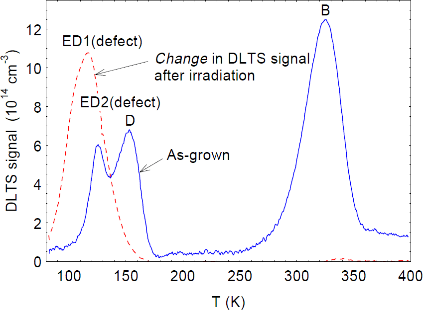
We now consider the use of DLTS to study point defects created by irradiation. The dashed line in figure 4 shows the change in the DLTS spectrum of a 4-μm-thick MOCVD GaN/Al2O3 layer after a 1-MeV electron irradiation to a fluence of 6 × 1015 cm−2. The only trap produced by the irradiation (in this DLTS temperature range) is the one designated E, with a peak near 115 K. It turns out that trap E is produced by several types of irradiation, including electrons [Reference Fang, Hemsky, Look and Mack8], protons [Reference Auret, Goodman, Koschnick, Spaeth, Beaumont and Gibart17], He ions [Reference Auret, Goodman, Koschnick, Spaeth, Beaumont and Gibart7], and sputtered Au atoms [Reference Auret, Goodman, Koschnick, Spaeth, Beaumont and Gibart18], and thus must be a rather common point defect. The usual Arrhenius analysis of E gives energies ranging from 0.13 to 0.20 eV, depending on the type of irradiation [Reference Auret, Goodman, Koschnick, Spaeth, Beaumont and Gibart7,Reference Fang, Hemsky, Look and Mack8,Reference Auret, Goodman, Koschnick, Spaeth, Beaumont and Gibart17,Reference Auret, Goodman, Koschnick, Spaeth, Beaumont and Gibart18]; however, very recently it has been shown that trap E, or at least the version produced by 1-MeV electrons, really consists of two traps, ED1 and ED2, as shown in figure 5 [Reference Polenta, Fang and Look19]. (Note that trap D in this spectrum existed before the irradiation.) Both ED1 and ED2 have thermal energies of 0.06 eV, identical to that of the donor found from the TDH measurements; however, they have different capture cross sections, with that of ED2 being temperature dependent. It is likely that ED1 and ED2 are both related to VN, but that, in fact, they are different complexes of VN. For example, one of them could be VN-NI, and the other, VN-NGa-GaN-NI. That is, from a simple theoretical model, presented in reference 20, each of these “chain” defect complexes could be produced by 1-MeV electrons. At a low enough irradiation energy, it should be possible to produce only the VN-NI defect, if it is stable at room temperature, and the presence of only one defect would simplify the analysis. At present, an “exact” analysis, such as that shown in figure 5, is absolutely essential to understand the important relationship between the irradiationproduced DLTS and TDH centers.

Figure 4. DLTS spectra for an as-grown MBE GaN layer (solid line), and an irradiated MOCVD GaN layer (dashed line). The spectrum for the irradiated sample actually represents only the change due to irradiation.
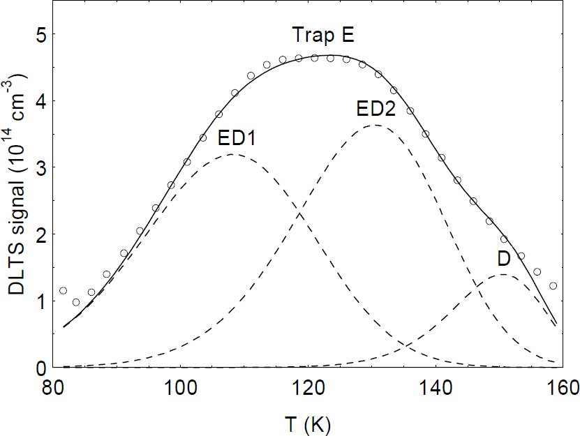
Figure 5. DLTS spectrum of Trap E. The solid line is the composite signal resulting from the three simulated traps shown as dashed lines.
The practical importance of trap E becomes obvious when comparing with the DLTS spectrum of an as-grown MBE GaN/Al2O3 layer, also shown in figure 4. Note that the as-grown layer contains trap ED2, at a reasonably high concentration. There is independent evidence that trap ED2 (called E1 in reference 21) is reduced by using higher N fluxes in the growth; this information is consistent with the VN nature of trap E.
By going to higher DLTS temperatures, another irradiation-induced trap appears, trap AD2, as shown in figure 2. The energy of trap AD2 is about 0.9 eV, close to that of a photoluminescence band which appears in electron-irradiated GaN, and which has tentatively been assigned to a GaI-X complex [Reference Linde, Uftring, Watkins, Härle and Scholz22]. Interestingly, the as-grown MBE GaN layer shown in figure 2 displays trap A1, which also has an energy of about 0.9 eV, and may be related to the defect trap AD2. (Trap A1 also appears in MOCVD and HVPE layers.) Traps ED2 and AD2 may be expected to influence GaN devices, because these traps can reach levels of 1015 cm−3 or higher in some samples.
Another point defect which has been studied in as-grown GaN is the Ga vacancy, VGa. Theory suggests that VGa centers should be prevalent in n-type GaN [Reference Neugebauer and Van de Walle3], and indeed, they have been identified by positron annihilation experiments [Reference Saarinen, Nissilä, Hautojärvi, Likonen, Suski, Grzegory, Lucznik and Porowski23]. It is a mystery as to why the VGa defect has not yet been found in irradiated GaN, but the VGa-GaI Frenkel pairs possibly recombine as soon as they are created, in n-type material, due to the strong coulomb attraction between VGa 3− and GaI +.
The results presented here show that point defects in GaN can be donors, acceptors, traps, and recombination centers, and that they exist in as-grown GaN layers. Although not specifically discussed in this paper, it is also important to note that defects will be produced in a radiation environment, such as that associated with the Van Allen belt. Future tasks include showing how point defects may affect particular types of devices, and then, how to get rid of them. This program is likely to engage the GaN community for some time to come.
Summary
Three types of defects, point, line, and areal, have been found in n-type GaN, and can influence the electrical properties of the material. Line defects, namely threading dislocations, have been shown to act as acceptors, recombination centers, scattering centers, and possibly traps, while areal defects, stacking faults in this case, induce a highly conductive interface region in HVPE GaN/Al2O3 layers. We have employed high-energy electron irradiation to create point defects, and have used TDH and DLTS to show that at least one of them is a donor, and that two of them are traps. We have also shown that very similar traps exist in as-grown GaN layers, and may have an effect on GaN devices.
Acknowledgements
We wish to thank H. Morkoç and R. Molnar for samples; S. Keller for raw, Hall data; and J.W. Hemsky for electron irradiations. D.C.L. and Z-Q. F. were supported under U.S. Air Force Contract F33615-95-C-1619 and U.S. Navy Grant N00014-99-1-1067. LP was supported by INFM (Italian National Institute for Physics of Matter). Also, partial support was received from the Air Force Office of Scientific Research. Most of the work of D.C.L. was performed at the Air Force Research Laboratory, Wright-Patterson Air Force Base, Ohio.