


Introdution
Recent progresses in III-nitride material growth and device processing have greatly extended their applications in the area of electronic as well as optoelectronic devices [Reference Morkoc, Strite, Gao, Lin, Sverdlov and Burns1,Reference Mohammad, Salvador and Morkoc2]. For electronic device applications, AlxGa1−xN/GaN heterojunction field-effect transistors (HFETs) have shown great promises in microwave and millimeter-wave electronic device applications [Reference Khan, Shur, Kuznia, Chen, Burn and Schaff3-Reference Wu, Keller, Fini, Keller, Jenkins, Kehias and DenBaars5]. However, the performance of AlGaN/GaN HFETs still falls far from that of the theoretical prediction [Reference Gelmont, Kim and Shur6]. Further improvements in AlGaN/GaN heterojunction material quality as well as in structural design are needed. Routine but powerful material and device characterization methods must be established.
In this work, Al0.25Ga0.75N/GaN modulation-doped heterojunction field-effect transistor (MOD-HFET) structures grown on sapphire substrates have been produced by our metal organic chemical vapor deposition (MOCVD) system and characterized by Hall and persistent photoconductivity measurements. The persistent photoconductivity (PPC) effect, which has been observed previously in GaN materials by several groups [Reference Johnson, Lin, Jiang, Khan and Sun7-Reference Li, Lin, Jiang, Khan and Chen11], was universally presented in these AlGaN/GaN HFET structures, indicating the presence of charge trapping effects. However, the magnitude of the PPC was observed to be a strong function of only one parameter, the product of sheet carrier density (ns ) and the two-dimensional electron gas mobility (μ). Since nsμ is the most important intrinsic material parameter for the HFET structural design, the magnitude of PPC in turn can be utilized as a sensitive probe for monitoring the electronic qualities of the AlGaN/GaN MOD-HFET structures.
Experimental Details
The inset of Fig. 1 is a schematic diagram showing the generic structure of samples used in this work which consisted of a 1.3 μm highly insulating GaN epilayer followed by an Al0.25Ga0.75N spacer layer and finally a Si-doped Al0.25Ga0.75N layer. The structures were deposited over basal plane sapphire substrates using a variable pressure MOCVD system at a growth temperature of 1050 0C. A total of seven samples with varying growth or structural parameters were studied. For the PPC measurements, a 1.5 V bias was supplied to the sample, a Hg lamp was used as an excitation source, and the conductivity was monitored through current (Ippc ) by using an electrometer. To ensure that each set of data obtained under different temperatures have the same initial conditions, the system was always heated up to 300 K, then cooled down in darkness to the desired measurement temperatures. The excitation intensity and buildup time span are fixed for different temperatures and samples. Fig. 1 illustrates the temperature variations of the sheet carrier density and mobility for one of our optimized structures. The values of the sheet carrier density and mobility products (nsμ) at different temperatures shown in Fig. 1 are among those highest values reported for the AlGaN/GaN HFET structures grown on sapphire substrates [Reference Gaska, Shur, Bykhovski, Orlov and Snider12-Reference Elsass, Smorchkova, Heying, Haus, Fini, Maranowski, Ibbetson, Keller, Petroff, DenBaars, Mishra and Speck14].
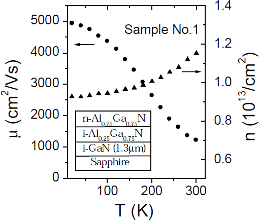
Fig. 1 2DEG sheet carrier density (ns ) and mobility (μ) versus temperature, T, measured in a dark state for one of our optimized Al0.2Ga0.8N/GaN MOD-HFET structures. The inset shows the generic structures for the samples used in this study.
For all seven structures investigated here, the conductivity of the 2DEG channel is enhanced after exposure to light. Moreover, the light enhanced conductivity persists for a long period of time after the removal of excitation source, an effect which is referred to as PPC. In Fig. 2, we present the PPC results obtained for three representative samples measured at two different temperatures. We can see that the decay time constants of the low temperature PPC are very long. By formulating the PPC buildup and decay kinetics in an AlGaN/GaN heterostructure, we have previously attributed the PPC effect to the photoionization of deep level centers in AlGaN barrier [Reference Li, Lin, Jiang, Khan and Chen11]. It is well known from the earlier works on the AlGaAs/GaAs MODFETs that the PPC effects are detrimental to their performance [Reference Mooney15]. The effects include sensitivity to light, a shift of the threshold voltage, and collapse of the drain I-V characteristics, all of which reduced the usefulness of the AlGaAs/GaAs MODFET for integrated circuits. Interestingly, for AlGaN/GaN HFET structures studied here, we observe that the magnitude of PPC and hence the device instabilities can be minimized by varying the growth conditions as well as structural parameters. Table 1 summarizes our Hall and PPC measurement results for all seven structures with different structural and growth parameters. As shown in Table 1, the magnitude of PPC or the photoinduced conductivity enhancement (Ippc − Id ) over its dark level (Id ) is about 200% in sample #7, but is negligibly small (only about 3%) in sample #1.
Table 1. Hall-effect and PPC measurement results of the seven Al0.25Ga0.75N/GaN MODHFET structures obtained at 20 K and 300 K, together with the structural parameters (spacer and Si-doped AlGaN layer thicknesses), the relative Si-doping levels (SiH4 flow rate), and the growth pressure. All structures were grown at 1050 °C in a variable pressure MOCVD. Here Ippc denotes the buildup levels of the persistent currents for a fixed excitation intensity and buildup time span and Id the initial dark current levels.
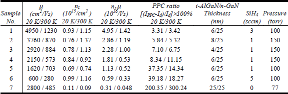
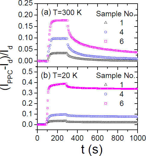
Fig. 2 Buildup and decay kinetics of PPC associated with the 2DEG system in three Al0.25Ga0.75N/GaN MOD-HFET structures measured at two representative temperatures, (a) T = 300 K and (b) T = 20 K. Here I ppc denotes the persistent photocurrent measured at time t and I d the initial dark current levels.
The general trends shown in Table 1 are that samples possess higher mobilities as well as higher sheet carrier densities exhibit reduced PPC, however, with a few exceptions (e.g., samples #4 & #5). By carefully inspecting the results summarized in Table 1, we can clearly see that the magnitude of PPC has a systematic dependence only on the product of the 2DEG sheet carrier density and mobility, i.e., nsμ, the most important intrinsic material parameter for the HFET device design. In Fig. 3, we have re-plotted the the magnitude of PPC versus nsμ measured at 20 K (a) and 300 K (b). At both temperatures, the magnitude of PPC decreases monotonously with an increase of nsμ, follows the relationship of
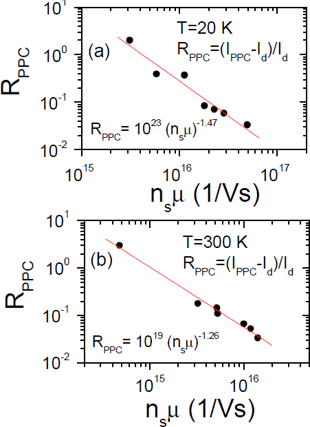
Fig. 3 The magnitude of PPC, Rppc , or the photoinduced conductivity enhancement for a fixed excitation intensity and buildup time span (Ippc − Id ) over its dark level (Id ) as a function of the product of the sheet carrier density and mobility, nsμ, obtained from seven different HFET structures. The solid lines are the least squares fits to experimental data with Rppc = A(nsμ)−α. The fitted values of α (A) are 1.47 (1023) and 1.26 (1019) at 20 K and 300 K, respectively.
Here the magnitude of PPC (Rppc ) is defined as [(Ippc − Id )/Id ] and A and α are two constants. As illustrated in Table 1, the better structures (i.e., larger values of nsμ) were achieved by varying (i) the AlGaN space layer thickness, (ii) the Si-doped AlGaN layer thickness, (iii) the doping levels in the Si-doped AlGaN layer, and (iv) the growth pressure. The electronic qualities (or nsμ values) of these HFET structures can be further improved slightly by adjusting the four parameters described above until the magnitude of PPC further reduces to zero. However, we speculate that further dramatic enhancements in AlGaN/GaN heterostructure material quality require further enhancements in epitaxial film qualities of both the underlying i-GaN and the top AlGaN epilayers.
The strong PPC effect observed in several samples here is associated with both the photoinduced increases in 2DEG sheet carrier density and mobility. In these structures, the sheet carrier densities at fixed temperatures in a single sample can be continuously varied by varying the excitation photon dose, while the increases in sheet carrier densities also result in enhancements in 2DEG mobilities. Such behaviors have been seen previously in an AlGaN/GaN HFET structure [Reference Li, Lin, Jiang, Khan and Chen11], which clearly demonstrates that one of the possible ways to enhance the 2DEG mobilities is to increase the sheet carrier densities in the 2DEG channel region. In desired structures with minimal PPC effects, enhanced mobilities can be accomplished by barrier or channel doping. However, at much greater sheet carrier densities, the population of the higher-lying subbands could limit the overall mobility of the structure due to intersubband scattering as well as the loss of the true two-dimensional behavior due to a virtual continuum of bands being populated [Reference Gaska, Shur, Bykhovski, Orlov and Snider12,Reference Dang, Asbeck, Yu, Sullivan, Chen, McDermott, Bouttros and Redwing16,Reference Hsu and Walukiewicz17]. Thus a trade-off between these effects must be considered.
In summary, we have shown in this work that the most important intrinsic material parameter for the AlGaN/GaN HFET device design, namely the sheet carrier and mobility product (nsμ) is strongly correlated with the magnitude of PPC in these structures. As a result, the magnitude of PPC can be utilized as a sensitive probe for monitoring the electronic qualities of the AlGaN/GaN MOD-HFET structures. We observed that the magnitude of the PPC and hence the photoinduced instability associated with these heterostructures decreases rapidly with an increase of nsμ, according to Rppc ∝ (nsμ)−α, withα varying from 1.26 to 1.47 in the temperature range of 20 to 300 K.
Acknowledgements
This research is supported by BMDO (Dr. Kepi Wu) monitored by USASSDC, NSF (DMR-99502431), and DOE(DE-FG03-96ER45604).


