Hostname: page-component-848d4c4894-xm8r8 Total loading time: 0 Render date: 2024-07-03T22:18:34.921Z Has data issue: false hasContentIssue false

Wet chemical etching of cadmium telluride photovoltaics for enhanced open-circuit voltage, fill factor, and power conversion efficiency

Published online by Cambridge University Press:  09 December 2019

Ebin Bastola
Affiliation:
Wright Center for Photovoltaics Innovation and Commercialization (PVIC), Department of Physics and Astronomy, University of Toledo, Toledo, Ohio 43606, USA
Fadhil K. Alfadhili
Affiliation:
Wright Center for Photovoltaics Innovation and Commercialization (PVIC), Department of Physics and Astronomy, University of Toledo, Toledo, Ohio 43606, USA
Adam B. Phillips
Affiliation:
Wright Center for Photovoltaics Innovation and Commercialization (PVIC), Department of Physics and Astronomy, University of Toledo, Toledo, Ohio 43606, USA
Michael J. Heben
Affiliation:
Wright Center for Photovoltaics Innovation and Commercialization (PVIC), Department of Physics and Astronomy, University of Toledo, Toledo, Ohio 43606, USA
Randy J. Ellingson*
Affiliation:
Wright Center for Photovoltaics Innovation and Commercialization (PVIC), Department of Physics and Astronomy, University of Toledo, Toledo, Ohio 43606, USA
*
a)Address all correspondence to this author. e-mail: Randy.Ellingson@utoledo.edu
Get access

Abstract

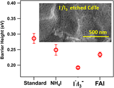
Cadmium telluride (CdTe) is one of the leading photovoltaic technologies with a market share of around 5%. However, there still exist challenges to fabricate a rear contact for efficient transport of photogenerated holes. Here, etching effects of various iodine compounds including elemental iodine (I2), ammonium iodide (NH4I), mixture of elemental iodine and NH4I (I/I3 etching), and formamidinium iodide were investigated. The treated CdTe surfaces were investigated using Raman spectroscopy, X-ray diffraction (XRD), scanning electron microscopy, and energy-dispersive X-ray spectroscopy. The CdTe devices were completed with or without treatments and tested under simulated AM1.5G solar spectrum to find photoconversion efficiency (PCE). Based on Raman spectra, XRD patterns, and surface morphology, it was shown that treatment with iodine compounds produced Te-rich surface on CdTe films, and temperature-dependent current–voltage characteristics showed reduced back barrier heights, which are essential for the formation of ohmic contact and reduce contact resistance. Based on current–voltage characteristics, the treatment enhanced open-circuit voltage (VOC) up to 841 mV, fill factor (FF) up to 78.2%, and PCE up to 14.0% compared with standard untreated CdTe devices (VOC ∼ 814 mV, FF ∼ 74%, and PCE ∼ 12.7%) with copper/gold back contact.

Type
Invited Paper
Copyright
Copyright © Materials Research Society 2019 

Access options

Get access to the full version of this content by using one of the access options below. (Log in options will check for institutional or personal access. Content may require purchase if you do not have access.)

References

Duffy, N., Peter, L., and Wang, R.: Characterisation of CdS|CdTe heterojunctions by photocurrent spectroscopy and electrolyte electroreflectance/absorbance spectroscopy (EEA/EER). J. Electroanal. Chem. 532, 207 (2002).CrossRefGoogle Scholar
Munshi, A.H., Kephart, J., Abbas, A., Raguse, J., Beaudry, J-N., Barth, K., Sites, J., Walls, J., and Sampath, W.: Polycrystalline CdSeTe/CdTe absorber cells with 28 mA/cm2 short-circuit current. IEEE J. Photovolt. 8, 310 (2018).CrossRefGoogle Scholar
Paudel, N.R. and Yan, Y.: Enhancing the photo-currents of CdTe thin-film solar cells in both short and long wavelength regions. Appl. Phys. Lett. 105, 183510 (2014).CrossRefGoogle Scholar
Freeouf, J.L. and Woodall, J.M.: Schottky barriers: An effective work function model. Appl. Phys. Lett. 39, 727 (1981).CrossRefGoogle Scholar
Simonds, B.J., Palekis, V., Van Devener, B., Ferekides, C., and Scarpulla, M.A.: Pulsed laser induced ohmic back contact in CdTe solar cells. Appl. Phys. Lett. 104, 141604 (2014).CrossRefGoogle Scholar
Liyanage, G.K., Phillips, A.B., Alfadhili, F.K., Ellingson, R.J., and Heben, M.J.: The role of back buffer layers and absorber properties for >25% efficient CdTe solar cells. ACS Appl. Energy Mater. 2, 5419 (2019).CrossRefGoogle Scholar
Kumar, S.G. and Rao, K.K.: Physics and chemistry of CdTe/CdS thin film heterojunction photovoltaic devices: Fundamental and critical aspects. Energy Environ. Sci. 7, 45 (2014).CrossRefGoogle Scholar
Janik, E. and Triboulet, R.: Ohmic contacts to p-type cadmium telluride and cadmium mercury telluride. J. Phys. D: Appl. Phys. 16, 2333 (1983).CrossRefGoogle Scholar
Corwine, C.R., Pudov, A.O., Gloeckler, M., Demtsu, S.H., and Sites, J.R.: Copper inclusion and migration from the back contact in CdTe solar cells. Sol. Energy Mater. Sol. Cells 82, 481 (2004).Google Scholar
Bhandari, K.P., Tan, X., Zereshki, P., Alfadhili, F.K., Phillips, A.B., Koirala, P., Heben, M.J., Collins, R.W., and Ellingson, R.J.: Thin film iron pyrite deposited by hybrid sputtering/co-evaporation as a hole transport layer for sputtered CdS/CdTe solar cells. Sol. Energy Mater. Sol. Cells 163, 277 (2017).CrossRefGoogle Scholar
Phillips, A.B., Khanal, R.R., Song, Z., Zartman, R.M., DeWitt, J.L., Stone, J.M., Roland, P.J., Plotnikov, V.V., Carter, C.W., and Stayancho, J.M.: Wiring-up carbon single wall nanotubes to polycrystalline inorganic semiconductor thin films: Low-barrier, copper-free back contact to CdTe solar cells. Nano Lett. 13, 5224 (2013).CrossRefGoogle ScholarPubMed
Paudel, N.R. and Yan, Y.: Application of copper thiocyanate for high open-circuit voltages of CdTe solar cells. Prog. Photovoltaics 24, 94 (2016).CrossRefGoogle Scholar
Bhandari, K.P., Koirala, P., Paudel, N.R., Khanal, R.R., Phillips, A.B., Yan, Y., Collins, R.W., Heben, M.J., and Ellingson, R.J.: Iron pyrite nanocrystal film serves as a copper-free back contact for polycrystalline CdTe thin film solar cells. Sol. Energy Mater. Sol. Cells 140, 108 (2015).CrossRefGoogle Scholar
Bastola, E., Bhandari, K.P., and Ellingson, R.J.: Solution-processed nickel-alloyed iron pyrite thin film as hole transport layer in cadmium telluride solar cells. In IEEE 44th Photovoltaic Spec. Conf. (PVSC) (IEEE, Piscataway, 2017); pp. 738741.Google Scholar
Bastola, E., Bhandari, K.P., and Ellingson, R.J.: Application of composition controlled nickel-alloyed iron sulfide pyrite nanocrystal thin films as the hole transport layer in cadmium telluride solar cells. J. Mater. Chem. C 5, 4996 (2017).CrossRefGoogle Scholar
Bastola, E., Bhandari, K.P., Subedi, I., Podraza, N.J., and Ellingson, R.J.: Structural, optical, and hole transport properties of earth-abundant chalcopyrite (CuFeS2) nanocrystals. MRS Commun. 8, 970 (2018).CrossRefGoogle Scholar
Subedi, K.K., Bastola, E., Subedi, I., Song, Z., Bhandari, K.P., Phillips, A.B., Podraza, N.J., Heben, M.J., and Ellingson, R.J.: Nanocomposite (CuS)x(ZnS)1−x thin film back contact for CdTe solar cells: Toward a bifacial device. Sol. Energy Mater. Sol. Cells 186, 227 (2018).CrossRefGoogle Scholar
Li, J., Diercks, D.R., Ohno, T.R., Warren, C.W., Lonergan, M.C., Beach, J.D., and Wolden, C.A.: Controlled activation of ZnTe:Cu contacted CdTe solar cells using rapid thermal processing. Sol. Energy Mater. Sol. Cells 133, 208 (2015).CrossRefGoogle Scholar
Kurley, J.M., Panthani, M.G., Crisp, R.W., Nanayakkara, S.U., Pach, G.F., Reese, M.O., Hudson, M.H., Dolzhnikov, D.S., Tanygin, V., Luther, J.M., and Talapin, D.V.: Transparent ohmic contacts for solution-processed, ultrathin CdTe solar cells. ACS Energy Lett. 2, 270 (2017).CrossRefGoogle Scholar
Ochoa-Landín, R., Vigil-Galan, O., Vorobiev, Y.V., and Ramírez-Bon, R.: Chemically-deposited Te layers improving the parameters of back contacts for CdTe solar cells. Sol. Energy 83, 134 (2009).CrossRefGoogle Scholar
Song, T., Moore, A., and Sites, J.R.: Te layer to reduce the CdTe back-contact barrier. IEEE J. Photovolt. 8, 293 (2018).CrossRefGoogle Scholar
Niles, D.W., Li, X., Sheldon, P., and Höchst, H.: A photoemission determination of the band diagram of the Te/CdTe interface. J. Appl. Phys. 77, 4489 (1995).CrossRefGoogle Scholar
Watthage, S.C., Phillips, A.B., Liyanage, G.K., Song, Z., Gibbs, J.M., Alfadhili, F.K., Alkhayat, R.B., Ahangharnejhad, R.H., Almutawah, Z.S., and Bhandari, K.P.: Selective Cd removal from CdTe for high-efficiency Te back-contact formation. IEEE J. Photovolt. 8, 1125 (2018).CrossRefGoogle Scholar
Sarlund, J., Ritala, M., Leskelä, M., Siponmaa, E., and Zilliacus, R.: Characterization of etching procedure in preparation of CdTe solar cells. Sol. Energy Mater. Sol. Cells 44, 177 (1996).CrossRefGoogle Scholar
Ivanits’Ka, V., Moravec, P., Franc, J., Tomashik, Z., Feychuk, P., Tomashik, V., Shcherbak, L., Mašek, K., and Höschl, P.: Chemical etching of CdTe in aqueous solutions of H2O2–HI-citric acid. J. Electron. Mater. 36, 1021 (2007).CrossRefGoogle Scholar
Moravec, P., Ivanits’ka, V., Franc, J., Tomashik, Z., Tomashik, V., Mašek, K., Feychuk, P., Shcherbak, L., Höschl, P., and Grill, R.: Chemical interaction of CdTe and CdZnTe with aqueous solutions of H2O2-HI-tartaric acid. J. Electron. Mater. 38, 1645 (2009).CrossRefGoogle Scholar
Moravec, P., Tomashik, Z., Ivanits’Ka, V., Tomashik, V., Franc, J., Mašek, K., and Höschl, P.: Slow-polishing iodine-based etchant for CdTe and CdZnTe single crystals. J. Electron. Mater. 41, 2838 (2012).CrossRefGoogle Scholar
Ricco, A.J., White, H.S., and Wrighton, M.S.: X-ray photoelectron and Auger electron spectroscopic study of the CdTe surface resulting from various surface pretreatments: Correlation of photoelectrochemical and capacitance-potential behavior with surface chemical composition. J. Vac. Sci. Technol., A 2, 910 (1984).CrossRefGoogle Scholar
Bensouici, A., Carcelen, V., Plaza, J., De Dios, S., Vijayan, N., Crocco, J., Bensalah, H., Dieguez, E., and Elaatmani, M.: Study of effects of polishing and etching processes on Cd1−xZnxTe surface quality. J. Cryst. Growth 312, 2098 (2010).CrossRefGoogle Scholar
Ivanits’ka, V., Moravec, P., Franc, J., Tomashik, V., Tomashik, Z., Mašek, K., Chukhnenko, P., Höschl, P., and Ulrych, J.: Chemical polishing of CdTe and CdZnTe in iodine–methanol etching solutions. J. Electron. Mater. 40, 1802 (2011).CrossRefGoogle Scholar
Awni, R.A., Li, D.B., Grice, C.R., Song, Z., Razooqi, M.A., Phillips, A.B., Bista, S.S., Roland, P.J., Alfadhili, F.K., and Ellingson, R.J.: The effects of hydrogen iodide back surface treatment on CdTe solar cells. Sol. RRL 3, 1800304 (2019).CrossRefGoogle Scholar
Simonds, B.J., Meadows, H.J., Misra, S., Ferekides, C., Dale, P.J., and Scarpulla, M.A.: Laser processing for thin film chalcogenide photovoltaics: A review and prospectus. J. Photonics Energy 5, 050999 (2015).CrossRefGoogle Scholar
Koll, D.K., Taha, A.H., and Giolando, D.M.: Photochemical “Self-healing” pyrrole based treatment of CdS/CdTe photovoltaics. Sol. Energy Mater. Sol. Cells 95, 1716 (2011).CrossRefGoogle Scholar
Tessema, M.M. and Giolando, D.M.: Pinhole treatment of a CdTe photovoltaic device by electrochemical polymerization technique. Sol. Energy Mater. Sol. Cells 107(Suppl. C), 9 (2012).CrossRefGoogle Scholar
Niemegeers, A. and Burgelman, M.: Effects of the Au/CdTe back contact on IV and CV characteristics of Au/CdTe/CdS/TCO solar cells. J. Appl. Phys. 81, 2881 (1997).CrossRefGoogle Scholar
Phillips, A.B., Song, Z., DeWitt, J.L., Stone, J.M., Krantz, P.W., Royston, J.M., Zeller, R.M., Mapes, M.R., Roland, P.J., Dorogi, M.D., Zafar, S., Faykosh, G.T., Ellingson, R.J., and Heben, M.J.: High speed, intermediate resolution, large area laser beam induced current imaging and laser scribing system for photovoltaic devices and modules. Rev. Sci. Instrum. 87, 093708 (2016).CrossRefGoogle ScholarPubMed
Supplementary material: PDF

Bastola et al. supplementary material

Bastola et al. supplementary material

Download Bastola et al. supplementary material(PDF)
PDF 761.5 KB