Published online by Cambridge University Press: 19 October 2015

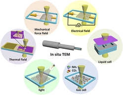
Two-dimensional (2D) materials, such as graphene, hexagonal boron nitride, and molybdenum sulfide (MoS2), have attracted considerable interest from the academia and industry because of their extraordinary properties. With the remarkable development of transmission electron microscope (TEM), nanolabs can be established inside the TEM to simulate a real environment by introducing external fields, such as electron irradiation, thermal excitation, electrical field, and mechanical force, into the system. In consequence, besides static structural characterization, in situ TEM can also realize dynamic observation of the evolution in structures and properties of 2D materials. This extension promises an enormous potential for manipulating and engineering 2D materials at the atomic scale with desired structures and properties for future applications. In this study, we review the recent progress of in situ electron microscopy studies of 2D materials, including atomic resolution characterization, in situ growth, nanofabrication, and property characterization.
Contributing Editor: Eric A. Stach
This paper has been selected as an Invited Feature Paper.