Hostname: page-component-76fb5796d-x4r87 Total loading time: 0 Render date: 2024-04-25T17:18:01.948Z Has data issue: false hasContentIssue false

Sequential multiplication of dislocation sources along a crack front revealed by high-voltage electron microscopy and tomography

Published online by Cambridge University Press:  11 March 2011

Masaki Tanaka*
Affiliation:
Department of Materials Science and Engineering, Kyushu University, Nishi-ku, Fukuoka 819-0395, Japan
Sunao Sadamatsu
Affiliation:
Department of Materials Science and Engineering, Kyushu University, Nishi-ku, Fukuoka 819-0395, Japan
Grace S. Liu
Affiliation:
Department of Materials Science and Engineering, University of Illinois, Urbana, Illinois 61801
Hiroto Nakamura
Affiliation:
Department of Materials Science and Engineering, Kyushu University, Nishi-ku, Fukuoka 819-0395, Japan
Kenji Higashida
Affiliation:
Department of Materials Science and Engineering, Kyushu University, Nishi-ku, Fukuoka 819-0395, Japan
Ian M. Robertson
Affiliation:
Department of Materials Science and Engineering, University of Illinois, Urbana, Illinois 61801
*
a)Address all correspondence to this author. e-mail: tanaka.masaki.760@m.kyushu-u.ac.jp
Get access

Abstract

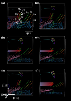
The three-dimensional structure of crack tip dislocations in single crystal silicon was observed by combining high-voltage electron microscopy and tomography. It was revealed that dislocations cross-slipped proximal to the crack tip even in the initial stages of plastic deformation. The local stress intensity factor along the crack front was calculated by taking into account the experimentally determined dislocation character. Based on these observations and calculations, a model to account for the sequential multiplication of dislocation sources along the crack front is proposed.

Type
Articles
Copyright
Copyright © Materials Research Society 2011

Access options

Get access to the full version of this content by using one of the access options below. (Log in options will check for institutional or personal access. Content may require purchase if you do not have access.)

Footnotes

b)

This author was an editor of this journal during the review and decision stages. For the JMR policy on review and publication of manuscripts authored by editors, please refer to http://www.mrs.org/jmr_policy

References

REFERENCES

1.St. John, C.: The brittle-to-ductile transition in pre-cleaved silicon single crystals. Philos. Mag. 32, 1193 (1975).Google Scholar
2.Brede, M. and Haasen, P.: The brittle-to-ductile transition in doped silicon as a model substance. Acta Metall. 36, 2003 (1988).CrossRefGoogle Scholar
3.Hirsch, P.B. and Roberts, S.G.: The brittle ductile transition in silicon. Philos. Mag., A 64, 55 (1991).CrossRefGoogle Scholar
4.de Oliveira, M.A.L. and Michot, G.: Three dimensional analysis of the interaction between a crack and a dislocation loop. Acta Mater. 46, 1371 (1998).CrossRefGoogle Scholar
5.Rice, J.R. and Thomson, R.: Ductile versus brittle behaviour of crystals. Philos. Mag. 29, 73 (1974).CrossRefGoogle Scholar
6.Thomson, R.: Brittle fracture in a ductile material with application to hydrogen embrittlement. J. Mater. Sci. 13, 128 (1978).CrossRefGoogle Scholar
7.Thomson, R.: Physics of fracture. In Solid State Physics, vol. 39; Seitz, F. and Turnbull, D., eds.; Academic Press: New York, 1986; p. 1.Google Scholar
8.Higashida, K. and Narita, N.: Crack tip plasticity and its role in the brittle-to-ductile transition. In JJAP Series 2, Lattice Defects in Ceramics. Suzuki, T. and Takeuchi, S., eds.; Japan Society of Applied Physics: Tokyo, 1989; p. 39.Google Scholar
9.Bulatov, V., Abraham, F.F., Kubin, L., Devincre, B., and Yip, S.: Connecting atomistic and mesoscale simulations of crystal plasticity. Nature 391, 669 (1998).CrossRefGoogle Scholar
10.Midgley, P.A., Weyland, M.W., Thomas, J.M., and Johnson, B.F.G.: Z-Contrast tomography: A technique in three-dimensional nanostructural analysis based on Rutherford scattering. Chem. Commun. 907 (2001).Google Scholar
11.Midgley, P.A. and Weyland, M.: 3D electron microscopy in the physical sciences: The development of Z-contrast and EFTEM tomography. Ultramicroscopy 96, 413 (2003).CrossRefGoogle ScholarPubMed
12.Kaneko, K., Nagayama, R., Inoke, K., Moon, W-J., Horita, Z., Hayashi, Y., and Tokunaga, T.: Formation of wedge-shaped carbon film by chemical vapor deposition method and observation using transmission electron microscopy. Scripta Mater. 52, 1205 (2005).CrossRefGoogle Scholar
13.Kimura, K., Hata, S., Matsumura, S., and Horiuchi, T.: Dark-field transmission electron microscopy for a tilt series of ordering alloys: Toward electron tomography. J. Electron Microsc. 54, 373 (2005).Google ScholarPubMed
14.Inoke, K., Kaneko, K., Weyl, M., Midgley, P.A., Higashida, K., and Horita, Z.: Severe local strain and the plastic deformation of Guinier–Preston zones in the Al–Ag system revealed by three-dimensional electron tomography. Acta Mater. 54, 2957 (2006).CrossRefGoogle Scholar
15.Barnard, J.S., Sharp, J., Tong, J.R., and Midgley, P.A.: High-resolution three-dimensional imaging of dislocations. Science 313, 319 (2006).CrossRefGoogle ScholarPubMed
16.Sharp, J.H., Barnard, J.S., Kaneko, K., Higashida, K., and Midgley, P.A.: Dislocation tomography made easy: A reconstruction from ADF STEM images obtained using automated image shift correction. J. Phys. Conf. Ser. 126, 012013 (2008).CrossRefGoogle Scholar
17.Tanaka, M., Higashida, K., Kaneko, K., Hata, S., and Mitsuhara, M.: Crack tip dislocations revealed by electron tomography in silicon single crystal. Scripta Mater. 59, 901 (2008).CrossRefGoogle Scholar
18.Barnard, J.S., Sharp, J., Tong, J.R., and Midgley, P.A.: Three-dimensional analysis of dislocation networks in GaN using weak-beam dark-field electron tomography. Philos. Mag. 86, 4901 (2006).CrossRefGoogle Scholar
19.Tanaka, M. and Higashida, K.: High-voltage electron-microscopical observation of crack-tip dislocations. Mater. Sci. Eng., A 400401, 426 (2005).CrossRefGoogle Scholar
20.Tanaka, M., Higashida, K., and Haraguchi, T.: Microstructure of plastic zones around crack tips in silicon revealed by HVEM and AFM. Mater. Sci. Eng., A 387389, 433 (2004).CrossRefGoogle Scholar
21.Higashida, K., Narita, N., Tanaka, M., Morikawa, T., Miura, Y., and Onodera, R.: Crack tip dislocations in silicon characterized by high-voltage electron microscopy. Philos. Mag., A 82, 3263 (2002).Google Scholar
22.Stanford university EM3D Home Page: http://em3d.stanford.edu/about/htmlGoogle Scholar
23.Ruvimov, S.S. and Scheerschmidt, K.: Burgers vector determination in TEM by using the dislocation parity analysis. Phys. Status Solidi. A 141, 269 (1994).CrossRefGoogle Scholar
24.Hirth, J.P. and Lothe, J.: Theory of Dislocations (McGraw–Hill, New York, 1986), pp. 1922.Google Scholar
25.Gao, H.: Crack interaction with 3-D dislocation loops. J. Mech. Phys. Solids 39, 157 (1991).CrossRefGoogle Scholar
26.Higashida, K., Narita, N., Asano, S., and Onodera, R.: Dislocation emission from a crack tip in MgO thin crystals. Mater. Sci. Eng., A 285, 111 (2000).CrossRefGoogle Scholar

Tanaka et al. supplementary material

Movie 1

Download Tanaka et al. supplementary material(Video)
Video 9.8 MB

Tanaka et al. supplementary material

Movie 2

Download Tanaka et al. supplementary material(Video)
Video 11.7 MB

Tanaka et al, supplementary material

Movie 3

Download Tanaka et al, supplementary material(Video)
Video 740.6 KB