


No CrossRef data available.
Article contents
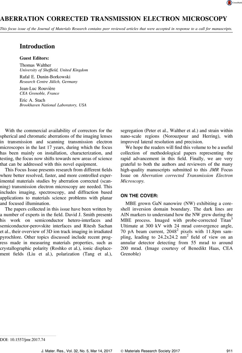
Introduction
Published online by Cambridge University Press: 14 March 2017
Abstract
An abstract is not available for this content so a preview has been provided. Please use the Get access link above for information on how to access this content.
- Type
- Aberration Corrected Transmission Electron Microscopy
- Information
- Journal of Materials Research , Volume 32 , Issue 5: Focus Issue: Aberration Corrected Transmission Electron Microscopy , 14 March 2017 , pp. 911
- Copyright
- Copyright © Materials Research Society 2017