


No CrossRef data available.
Article contents
In situ atomic level studies of thermally controlled interlayer stacking shifts in 2D transition metal dichalcogenide bilayers
Published online by Cambridge University Press: 13 January 2020
Abstract
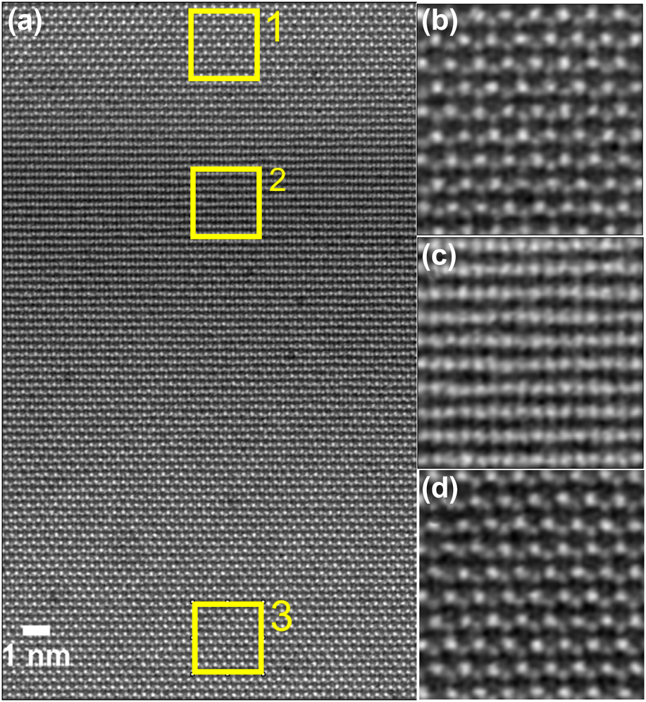
We show interlayer stacking shifts occur in transition metal dichalcogenides (TMD) bilayers due to the strain introduced during sample heating, and attributed to rippling of one layer relative to the other. The atomic structure of the interlayer stacking is studied using annular dark field scanning transmission electron microscopy with an in situ heating holder. Before heating, bilayers show uniform interlayer stacking of AA′ and AB. When heated, contrast change is seen and associated with interlayer stacking changes at the atomic scale due to ripples. When cooled down to room temperature, these contrast features disappear, confirming it is a reversible process that is not related to defects or vacancies. Because the bottom layer is attached to the in situ heating chip made from Si3N4 and the top layer is in contact with the underlying TMD layer with weak van der Waals interaction, the two layers experience different forces during thermal expansion.
- Type
- Invited Paper
- Information
- Journal of Materials Research , Volume 35 , Issue 11: Focus Section: Heterogeneity in Beyond Graphene 2D Materials , 15 June 2020 , pp. 1407 - 1416
- Copyright
- Copyright © Materials Research Society 2020
References
Ci, P., Chen, Y., Kang, J., Suzuki, R., Choe, H.S., Suh, J., Ko, C., Park, T., Shen, K., Iwasa, Y., and Tongay, S.: Quantifying van der Waals interactions in layered transition metal dichalcogenides from pressure-enhanced valence band splitting. Nano Lett. 17, 4982–4988 (2017).CrossRefGoogle Scholar
Splendiani, A., Sun, L., Zhang, Y., Li, T., Kim, J., Chim, C.Y., Galli, G., and Wang, F.: Emerging photoluminescence in monolayer MoS2. Nano Lett. 10, 1271–1275 (2010).10.1021/nl903868wCrossRefGoogle ScholarPubMed
He, J., Hummer, K., and Franchini, C.: Stacking effects on the electronic and optical properties of bilayer transition metal dichalcogenides MoS2, MoSe2, WS2, and WSe2. Phys. Rev. B 89, 075409 (2014).CrossRefGoogle Scholar
Li, H., Zhang, Q., Yap, C.C.R., Tay, B.K., Edwin, T.H.T., Olivier, A., and Baillargeat, D.: From bulk to monolayer MoS2: Evolution of Raman dcattering. Adv. Funct. Mater. 22, 1385–1390 (2012).CrossRefGoogle Scholar
Li, H., Yin, Z., He, Q., Li, H., Huang, X., Lu, G., Fam, D.W.H., Tok, A.I.Y., Zhang, Q., and Zhang, H.: Fabrication of single and multilayer MoS2 film-based field-effect transistors for sensing NO at room temperature. Small 8, 63–67 (2012).CrossRefGoogle ScholarPubMed
Late, D.J., Huang, Y.K., Liu, B., Acharya, J., Shirodkar, S.N., Luo, J., Yan, A., Charles, D., Waghmare, U.V., Dravid, V.P., and Rao, C.N.R.: Sensing behavior of atomically thin-layered MoS2 transistors. ACS Nano 7, 4879–4891 (2013).CrossRefGoogle ScholarPubMed
Liu, K., Zhang, L., Cao, T., Jin, C., Qiu, D., Zhou, Q., Zettl, A., Yang, P., Louie, S.G., and Wang, F.: Evolution of interlayer coupling in twisted molybdenum disulfide bilayers. Nat. Commun. 5, 4966 (2014).CrossRefGoogle ScholarPubMed
Van Der Zande, A.M., Kunstmann, J., Chernikov, A., Chenet, D.A., You, Y., Zhang, X., Huang, P.Y., Berkelbach, T.C., Wang, L., Zhang, F., and Hybertsen, M.S.: Tailoring the electronic structure in bilayer molybdenum disulfide via interlayer twist. Nano Lett. 14, 3869–3875 (2014).CrossRefGoogle ScholarPubMed
Suzuki, R., Sakano, M., Zhang, Y.J., Akashi, R., Morikawa, D., Harasawa, A., Yaji, K., Kuroda, K., Miyamoto, K., Okuda, T., and Ishizaka, K.: Valley-dependent spin polarization in bulk MoS2 with broken inversion symmetry. Nat. Nanotechnol. 9, 611 (2014).CrossRefGoogle ScholarPubMed
Wilson, J.A. and Yoffe, A.D.: The transition metal dichalcogenides discussion and interpretation of the observed optical, electrical and structural properties. Adv. Phys. 18, 193–335 (1969).CrossRefGoogle Scholar
Xia, M., Li, B., Yin, K., Capellini, G., Niu, G., Gong, Y., Zhou, W., Ajayan, P.M., and Xie, Y.H.: Spectroscopic signatures of AA' and AB stacking of chemical vapor deposited bilayer MoS2. ACS Nano 9, 12246–12254 (2015).10.1021/acsnano.5b05474CrossRefGoogle ScholarPubMed
Lee, J.U., Kim, K., Han, S., Ryu, G.H., Lee, Z., and Cheong, H.: Raman signatures of polytypism in molybdenum disulfide. ACS Nano 10, 1948–1953 (2016).10.1021/acsnano.5b05831CrossRefGoogle ScholarPubMed
Shmeliov, A., Shannon, M., Wang, P., Kim, J.S., Okunishi, E., Nellist, P.D., Dolui, K., Sanvito, S., and Nicolosi, V.: Unusual stacking variations in liquid-phase exfoliated transition metal dichalcogenides. ACS Nano 8, 3690–3699 (2014).CrossRefGoogle ScholarPubMed
Levita, G., Cavaleiro, A., Molinari, E., Polcar, T., and Righi, M.C.: Sliding properties of MoS2 layers: Load and interlayer orientation effects. J. Phys. Chem. C 118, 13809–13816 (2014).CrossRefGoogle Scholar
Xia, J., Zeng, Q., Zhou, J., Zhou, W., Zhang, Q., Yan, J., Liu, Z., and Shen, Z.X.: Current rectification and ssymmetric photoresponse in MoS2 stacking-induced homojunctions. 2D Mater. 4, 035011 (2017).CrossRefGoogle Scholar
Zhou, S., Wang, S., Shi, Z., Sawada, H., Kirkland, A.I., Li, J., and Warner, J.H.: Atomically sharp interlayer stacking shifts at anti-phase grain boundaries in overlapping MoS2 secondary layers. Nanoscale 10, 16692–16702 (2018).CrossRefGoogle ScholarPubMed
Lin, J., Fang, W., Zhou, W., Lupini, A.R., Idrobo, J.C., Kong, J., Pennycook, S.J., and Pantelides, S.T.: AC/AB stacking boundaries in bilayer graphene. Nano Lett. 13, 3262–3268 (2013).10.1021/nl4013979CrossRefGoogle ScholarPubMed
Brown, L., Hovden, R., Huang, P., Wojcik, M., Muller, D.A., and Park, J.: Twinning and twisting of tri-and bilayer graphene. Nano Lett. 12, 1609–1615 (2012).CrossRefGoogle ScholarPubMed
Hibino, H., Mizuno, S., Kageshima, H., Nagase, M., and Yamaguchi, H.: Stacking domains of epitaxial few-layer graphene on SiC(0001). Phys. Rev. B 80, 085406 (2009).10.1103/PhysRevB.80.085406CrossRefGoogle Scholar
Tapasztó, L., Dumitrică, T., Kim, S.J., Nemes-Incze, P., Hwang, C., and Biró, L.P.: Breakdown of continuum mechanics for nanometre-wavelength rippling of graphene. Nat. Phys. 8, 739 (2012).10.1038/nphys2389CrossRefGoogle Scholar
Brivio, J., Alexander, D.T., and Kis, A.: Ripples and layers in ultrathin MoS2 membranes. Nano Lett. 11, 5148–5153 (2011).CrossRefGoogle ScholarPubMed
Kushima, A., Qian, X., Zhao, P., Zhang, S., and Li, J.: Ripplocations in van der Waals layers. Nano Lett. 15, 1302–1308 (2015).CrossRefGoogle ScholarPubMed
Lui, C.H., Liu, L., Mak, K.F., Flynn, G.W., and Heinz, T.F.: Ultraflat graphene. Nature 462, 339 (2009).10.1038/nature08569CrossRefGoogle ScholarPubMed
Bonilla, L.L. and Carpio, A.: Model of ripples in graphene. Phys. Rev. B 86, 195402 (2012).CrossRefGoogle Scholar
Deng, S. and Berry, V.W.: Rippled and crumpled graphene: An overview of formation mechanism, electronic properties, and applications. Mater. Today 19, 197–212 (2016).10.1016/j.mattod.2015.10.002CrossRefGoogle Scholar
Vasić, B., Zurutuza, A., and Gajić, R.: Spatial variation of wear and electrical properties across wrinkles in chemical vapour deposition graphene. Carbon 102, 304–310 (2016).10.1016/j.carbon.2016.02.066CrossRefGoogle Scholar
Schiefele, J., Martin-Moreno, L., and Guinea, F.: Faraday effect in rippled graphene: Magneto-optics and random gauge fields. Phys. Rev. B 94, 035401 (2016).CrossRefGoogle Scholar
Liang, T., He, G., Wu, X., Ren, J., Guo, H., Kong, Y., Iwai, H., Fujita, D., Gao, H., Guo, H., and Liu, Y.: Permeation through graphene ripples. 2D Mater. 4, 025010 (2017).CrossRefGoogle Scholar
He, K., Poole, C., Mak, K.F., and Shan, J.: Experimental demonstration of continuous electronic structure tuning via strain in atomically thin MoS2. Nano Lett. 13, 2931–2936 (2013).CrossRefGoogle ScholarPubMed
Lin, Z., Carvalho, B.R., Kahn, E., Lv, R., Rao, R., Terrones, H., Pimenta, M.A., and Terrones, M.: Defect engineering of two-dimensional transition metal dichalcogenides. 2D Mater. 3, 022002 (2016).CrossRefGoogle Scholar
De Juan, F., Cortijo, A., and Vozmediano, M.A.: Charge inhomogeneities due to smooth ripples in graphene sheets. Phys. Rev. B 76, 165409 (2007).10.1103/PhysRevB.76.165409CrossRefGoogle Scholar
Herbut, I.F., Juričić, V., and Vafek, O.: Coulomb interaction, ripples, and the minimal conductivity of graphene. Phys. Rev. Lett. 100, 046403 (2008).CrossRefGoogle ScholarPubMed
Guinea, F., Horovitz, B., and Le Doussal, P.: Gauge field induced by ripples in graphene. Phys. Rev. B 77, 205421 (2008).CrossRefGoogle Scholar
Guinea, F., Horovitz, B., and Le Doussal, P.: Gauge fields, ripples and wrinkles in graphene layers. Solid State Commun. 149, 1140–1143 (2009).CrossRefGoogle Scholar
Guinea, F., Katsnelson, M.I., and Geim, A.K.: Energy gaps and a zero-field quantum Hall effect in graphene by strain engineering. Nat. Phys. 6, 30 (2010).CrossRefGoogle Scholar
Zhou, S., Wang, S., Li, H., Xu, W., Gong, C., Grossman, J.C., and Warner, J.H.: Atomic structure and dynamics of defects in 2D MoS2 bilayers. ACS Omega 2, 3315–3324 (2017).CrossRefGoogle ScholarPubMed
Tien, C.L. and Lin, T.W.: Thermal expansion coefficient and thermomechanical properties of SiNx thin films prepared by plasma-enhanced chemical vapor deposition. Appl. Opt. 51, 7229–7235 (2012).CrossRefGoogle Scholar
Gan, C.K. and Liu, Y.Y.F.: Direct calculation of the linear thermal expansion coefficients of MoS2 via symmetry-preserving deformations. Phys. Rev. B 94, 134303 (2016).CrossRefGoogle Scholar
Bano, A., Khare, P., and Gaur, N.K.: Thermal transport properties of bulk and monolayer MoS2: An ab initio approach. J. Phys.: Conf. Ser. 836, 012052 (2017).Google Scholar
Ding, Y. and Xiao, B.: Thermal expansion tensors, Grüneisen parameters and phonon velocities of bulk MT2 (M = W and Mo; T = S and Se) from first principles calculations. RSC Adv. 5, 18391–18400 (2015).CrossRefGoogle Scholar