Hostname: page-component-78c5997874-dh8gc Total loading time: 0 Render date: 2024-11-17T23:37:14.186Z Has data issue: false hasContentIssue false

Epitaxial growth and interfaces of high-quality InN films grown on nitrided sapphire substrates

Published online by Cambridge University Press:  16 April 2013

Fangliang Gao
Affiliation:
Department of Electronic Materials, State Key Laboratory of Luminescent Materials and Devices, South China University of Technology, Guangzhou 510640, China
Yunfang Guan
Affiliation:
Department of Electronic Materials, State Key Laboratory of Luminescent Materials and Devices, South China University of Technology, Guangzhou 510640, China
Jingling Li*
Affiliation:
Department of Electronic Materials, State Key Laboratory of Luminescent Materials and Devices, South China University of Technology, Guangzhou 510640, China
Junning Gao
Affiliation:
State Key Laboratory of Solidification Processing, Northwestern Polytechnical University, Xi’an 710072, China
Junqiu Guo
Affiliation:
Department of Electronic Materials, State Key Laboratory of Luminescent Materials and Devices, South China University of Technology, Guangzhou 510640, China
Guoqiang Li*
Affiliation:
Department of Electronic Materials, State Key Laboratory of Luminescent Materials and Devices, South China University of Technology, Guangzhou 510640, China
*
a)Address all correspondence to this author. e-mail: msgli@scut.edu.cn
Get access

Abstract

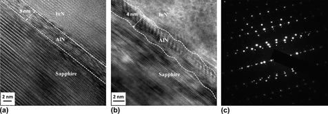
InN films have been grown on sapphire substrates nitrided by N plasma with different durations by radio-frequency plasma assisted molecular beam epitaxy (RF-MBE). In-depth investigation reveals that AlN is generated on a sapphire surface during the nitridation, and 60 min nitridation helps in the formation of an ordered and flat AlN interlayer between the substrate and the InN film, which improves the surface migration of In atoms on the substrate, and consequently helps in obtaining a single-crystalline c-plane InN film of high quality with 1.0 × 1019 cm−3 carrier density and 1350 cm2/(V·s) carrier mobility. Too short nitridation duration will result in a polycrystalline InN film, and too long nitridation duration will damage the surface quality of the newly generated AlN interlayer which consequently deteriorates the InN film quality. Control of the AlN interlayer quality plays a critical role in the growth of a high-quality InN epitaxial film on the sapphire substrate.

Type
Articles
Copyright
Copyright © Materials Research Society 2013 

Access options

Get access to the full version of this content by using one of the access options below. (Log in options will check for institutional or personal access. Content may require purchase if you do not have access.)

References

REFERENCES

Fu, S.P. and Chen, Y.F.: Effective mass of InN epilayers. Appl. Phys. Lett. 85, 1523 (2004).CrossRefGoogle Scholar
Polyakov, V.M. and Schwierz, F.: Low-field electron mobility in wurtzite InN. Appl. Phys. Lett. 88, 032101 (2006).CrossRefGoogle Scholar
Hurni, C.A., Choi, S., Bierwagen, O., and Speck, J.S.: Coupling resistance between n-type surface accumulation layer and p-type bulk in InN: Mg thin films. Appl. Phys. Lett. 100, 082106 (2012).CrossRefGoogle Scholar
Knuumlbel, A., Aidam, R., Cimalla, V., Kirste, L., Baeumler, M., Leancu, C.C., Lebedev, V., Wallauer, J., Walther, M., and Wagner, J.: Transport characteristics of indium nitride (InN) films grown by plasma assisted molecular beam epitaxy (PAMBE). Phys. Status Solidi C 6, 1480 (2009).Google Scholar
Hwang, J-S., Tsai, J-T., Lin, K-I., Lee, M-H., Tsai, C-N., Lin, H-W., Gwo, S., and Chen, M-C.: Terahertz radiation mechanism of native n-type InN with different carrier concentrations. Appl. Phys. Express 3, 102202 (2010).CrossRefGoogle Scholar
Metcalfe, G.D., Shen, H., Wraback, M., Koblmueller, G., Gallinat, C., Wu, F., and Speck, J.S.: Terahertz radiation from nonpolar InN due to drift in an intrinsic In-plane electric field. Appl. Phys. Express 3, 092201 (2010).CrossRefGoogle Scholar
Ahn, H., Yeh, Y.J., Hong, Y.L., and Gwo, S.: Terahertz emission mechanism of magnesium doped indium nitride. Appl. Phys. Lett. 95, 232104 (2009).CrossRefGoogle Scholar
Wang, X.Q., Zhao, G.Z., Zhang, Q., Ishitani, Y., Yoshikawa, A., and Shen, B.: Effect of Mg doping on enhancement of terahertz emission from InN with different lattice polarities. Appl. Phys. Lett. 96, 061907 (2010).CrossRefGoogle Scholar
Hangleiter, A.: III-V nitrides: A new age for optoelectropics. MRS Bull. 28, 350 (2003).CrossRefGoogle Scholar
Trybus, E., Namkoong, G., Henderson, W., Burnham, S., Doolittle, W.A., Cheung, M., and Cartwright, A.: InN: A material with photovoltaic promise and challenges. J. Cryst. Growth 288, 218 (2006).CrossRefGoogle Scholar
Hovel, H.J. and Cuomo, J.J.: Electrical and optical properties or rf-sputtered GaN and InN. Appl. Phys. Lett. 20, 71 (1972).CrossRefGoogle Scholar
Song, D.Y., Kuryatkov, V., Basavaraj, M., Rosenbladt, D., Nikishin, S.A., Holtz, M., Syrkin, A.L., Usikov, A.S., Ivantsov, V.A., and Dmitriev, V.A.: Morphological, electrical, and optical properties of InN grown by hydride vapor phase epitaxy on sapphire and template substrates. J. Appl. Phys. 99, 116103 (2006).CrossRefGoogle Scholar
Rauch, C., Tuna, O., Giesen, C., Heuken, M., and Tuomisto, F.: Point defect evolution in low-temperature MOCVD growth of InN. Phys. Status Solidi A 209, 87 (2012).CrossRefGoogle Scholar
Kuyyalil, J., Tangi, M., and Shivaprasad, S.M.: Dependence of crystal orientation and bandgap on substrate temperature of molecular-beam epitaxy grown InN on bare Al2O3 (0001). J. Appl. Phys. 109, 093513 (2011).CrossRefGoogle Scholar
Stokker-Cheregi, F., Nedelcea, A., Filipescu, M., Moldovan, A., Colceag, D., Ion, V., Birjega, R., and Dinescu, M.: High temperature growth of InN on various substrates by plasma-assisted pulsed laser deposition. Appl. Surf. Sci. 257, 5312 (2011).CrossRefGoogle Scholar
Li, G. and Yang, H.: Epitaxial growth of high quality nonpolar InN films on LiGaO2 substrates. Cryst. Growth Des. 11, 664 (2011).CrossRefGoogle Scholar
Huang, Q., Li, S., Cai, D., and Kang, J.: Kinetic behavior of nitrogen penetration into indium double layer improving the smoothness of InN film. J. Appl. Phys. 111, 113528 (2012).CrossRefGoogle Scholar
Lu, H., Schaff, W.J., Eastman, L.F., and Stutz, C.E.: Surface charge accumulation of InN films grown by molecular-beam epitaxy. Appl. Phys. Lett. 82, 1736 (2003).CrossRefGoogle Scholar
Klochikhin, A.A., Davydov, V.Y., Strashkova, I.Y., and Gwo, S.: Classical and quantum solutions of the planar accumulation layer problem within the parabolic effective-mass approximation. Phys. Rev. B 76, 235325 (2007).CrossRefGoogle Scholar
Mahboob, I., Veal, T.D., McConville, C.F., Lu, H., and Schaff, W.J.: Intrinsic electron accumulation at clean InN surfaces. Phys. Rev. Lett. 92, 036804 (2004).CrossRefGoogle ScholarPubMed
Bhuiyan, A.G., Hashimoto, A., and Yamamoto, A.: Indium nitride (InN): A review on growth, characterization, and properties. J. Appl. Phys. 94, 2779 (2003).CrossRefGoogle Scholar