


Introduction
Modern wireless communication and radar systems require multi-purpose, multi-standard, and multi-frequency radio frequency (RF) front-ends that can operate in the presence of strong interference. This requirement is due to rapid increase of various systems, standards, and co-existing in the same spectrum. As a result there is a significant interest in multi-band bandpass filters (BPF), particularly dual-band filters. Additionally, future communication systems are shifting towards higher-frequencies, in the range of microwave to millimeter-wave. Conventionally, dual-band filters in the microwave regime have been designed using substrate integrated waveguide (SIW) cavities and/or microstrip lines [Reference Li, Chen and Chen1–Reference Shen, Wang, Kang and Wu7] which are not practical to integrate on chip. These solutions also typically lack tuning capabilities, and therefore, multiple switched filters are needed to cover different frequency bands. The cost and form factor of such solution thereby increases significantly. Numerous off-chip techniques to obtain dual-band response have been proposed in [Reference Li, Chen and Chen1,Reference Liu, Katehi and Peroulis3–Reference Shen, Wang, Kang and Wu7] including stepped impedance resonator, capacitively loaded dual cavity resonators, and microstrip-based coupled resonating sections. An off-chip passive tunable multiband BPF covering 0.8–1.2 GHz, employing Wilkinson type power divider [Reference Psychogiou, Gómez-García, Guyette and Peroulis2], has been reported with good performance but with limited integration capability and large area. To date, no work has been reported for on-chip dual-band operation at higher microwave frequencies. For cost effective multiband systems, one practical solution is to use minimal off-chip bulky filters with a wide pass-band coverage, in conjunction with on-chip tunable filter to reject the out-of-band (OOB) interferers further.
Recent developments in on-chip filtering include N-path and Q-enhanced LC filters [Reference Kibaroglu and Rebeiz8–Reference Hwu and Razavi12]. N-path filters typically employ a wideband low-noise amplifier followed by a narrowband frequency tunable filtering [Reference Kibaroglu and Rebeiz8,Reference Chen and Hashemi10–Reference Hwu and Razavi12] using switches driven by N no. of multi-phase clocks. These filters, however, are mostly limited to lower RF frequencies (below ~3 GHz) and their filtering performance degrades as frequency increases. This degradation is due to switch parasitics which limit theOOB attenuation as well as inaccurate multi-phase clock generation at higher frequencies with associated large power consumption. For example in [Reference Shen, Wang, Kang and Wu7], at the expense of significant power consumption, the OOB attenuation is still limited to 20 dB or worse at frequencies above 10 GHz in CMOS SOI 32 nm.
Compared with N-path filters, Q-enhanced LC filtering is quite suitable at higher microwave frequencies due to increased on-chip inductor Qs and reduced size [Reference Mohammadi and Koh9,Reference Amin, Raman and Koh13]. Additionally Q-enhanced LC filtering provides increased OOB attenuation, and potential for fast frequency tuning.
In this paper, an on-chip Q-enhanced dual-band filtering solution based on prior work single-band tunable designs is presented along with measured results at microwave frequencies. The section “Synthetic parallel dual-Band filtering” introduces the parallel synthesis technique and analysis. The section “Circuit design and implementation” covers detailed implementation followed by measurement results in the section “Measurement results”. Finally, the section “Conclusion” concludes this work.
Synthetic parallel dual-band filtering
Figure 1 shows the concept of parallel synthesis techniques using two LC-tanks. The center frequencies of the LC-tanks are tunable using the varactors C. The Q of the LC-tank can be tuned using a variable load resistance R P. By exploiting the LC-tank's phase characteristics, two types of dual-band band-pass shaping are achievable. The first characteristic is achieved by subtracting the two LC-tank responses with largely spaced center frequencies ω 01 and ω 02 to form a dual-band filter response with higher OOB attenuations. However, between bands the attenuation is 6 dB less compared with the 2nd-order BPF responses alone. This can be explained by the phase changes of the two LC-tanks where both LC-tanks are inductive below the center frequency ω 01 of BPF1 and therefore, are in phase. When the responses are subtracted in this region the resulting roll-off will be steeper than the 2nd BPFs alone. The same is true for the region higher than the center frequency ω 02 of BPF2. In between the two center frequencies ω 01 and ω 02, BPF1 is capacitive whereas BPF2 is inductive; hence, they are out-of-phase resulting in addition of the waveforms when the outputs are subtracted. The second characteristic is achieved by adding the two LC-tank responses. This results in a sharp notch between the two center frequencies for higher attenuation between the bands. However, the ultimate rejection levels on the higher and lower sides of the center frequency worsen by 6 dB compared with individual 2nd-order BPF responses due to additive common impedance by the two BPFs. The choice of addition or subtraction to form dual-band responses depends on the application and operating frequencies; nevertheless, a trade-off exists between in-band attenuation versus OOB attenuation. The addition mode resulting in the deeper notch may be desirable at lower RF frequencies where an attenuation in-between the bands is important. The subtraction mode is favorable, in general, at higher microwave frequencies where the band separations are larger. To find the attenuation in-between bands, the 2nd-order transfer function can be expressed as
 $$H(s)= \displaystyle{{\omega_0 \over Q}s \over s^2+\displaystyle{\omega_0 \over Q}s+\omega_0^2}$$
 $$H(s=j\omega)= {1 \over 1+jQ\displaystyle{\left({\omega \over \omega_0}-{\omega_0 \over \omega}\right)}},$$
for large Q, (2) can be expressed as
 $$\mid H(\,j\omega)\mid \approx {1 \over Q \displaystyle{\left({\omega \over \omega_0}-{\omega_0 \over \omega}\right)}} .$$
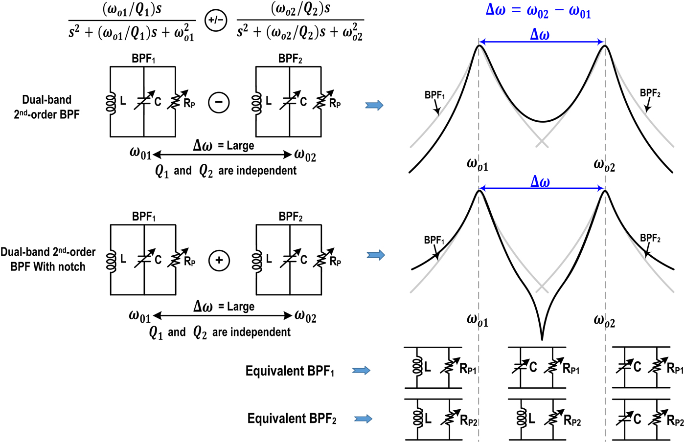
Fig. 1. Shaping of dual-bands BPF responses by parallel synthesis of two tunable (Q and center-frequency) LC-tanks.
To find attenuation between bands by the first BPF, substitute ω 0 = ω 01 and 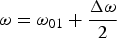 $\omega =\omega _{01}+ {\Delta \omega \over 2}$, and after approximation, (3) can be expressed as
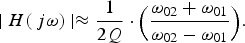 $$\mid H(\,j\omega)\mid \approx {1 \over 2Q}\cdot \Big( {\omega_{02}+\omega_{01} \over \omega_{02}-\omega_{01}} \Big ).$$
Therefore, for the same Q of each band, the total attenuation between bands will be added and can be expressed in dB as
 $$A_T=20 \; log \displaystyle{\left( {1 \over 2Q} \cdot { (\omega_{02}+\omega_{01}) \over (\omega_{02} - \omega_{01})} \right)}+6(dB),$$
where ω 01 and ω 02 are the center frequencies of LC-tanks. This shows that the in-between bands attenuation is degraded by 6 dB compared with a 2nd-order BPF response.
Figure 2(a) shows the simulation and the approximate relation derived in (5) against the frequency spacing between the two bands in terms of ratio of ω 02–ω 01. In this case, the Q of each BPF is 50 and the spacing between the two bands are varied from very small to when ω 02 is twice that of ω 01. The plots shows agreement between the simulation and the theoretical approximation. The relation in (5) can reveal important design parameters in terms of Q and spacing between the two bands to achieve a targeted attenuation. For example, when Q of both bands is set to 50, the spacing resulting in ω 02 = 1.5ω 01 guarantees at least 20 dB of attenuation.
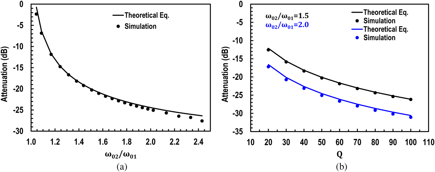
Fig. 2. (a) In-between bands attenuation for theoretical approximate equation and simulation (a) versus dual-band frequencies ratio and (b) versus Q of the each dual bands.
Figure 2(b) shows the plots of theoretical equation and simulation versus Q of the two bands for two cases of ω 02 and ω 01 spacing. For the Q of 100 of each band, the attenuation is more than 31 dB when ω 02 is twice that of ω 01. An ideal lumped components simulation with dual-bands around 10 and 14 GHz each having 200 MHz of bandwidth (BW) is shown in Fig. 3. The trade-off between in-between bands and OOB attenuation is evident for the two synthesis cases of addition and subtraction. Note the OOB attenuation on higher side of the 14 GHz for the case of subtraction compared with addition, thus mitigating the effects of less roll-off of BPF. As proof of concept of this approach, the subtraction mode was demonstrated using the design of [Reference Amin, Raman and Koh13].
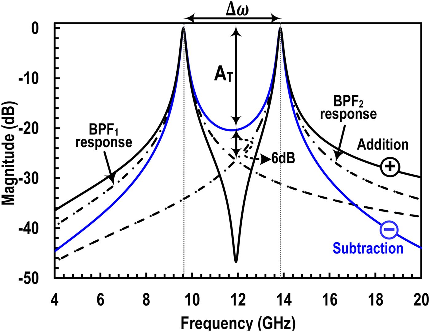
Fig. 3. Ideal lumped circuit simulations of dual-band BPF at 9.7 and 13.9 GHz.
Circuit design and implementation
The proposed parallel synthesis techniques requires independent tuning of the center frequency and Q of the LC-tanks. Figure 4(a) shows the block diagram of the proposed filter where two tunable 2nd-order BPFs outputs are subtracted using transistors (Q A−B) and (Q C−D) and resistor R 0 and R E. Resistance R 0 also serves to match to 50 Ω output for measurement purposes.
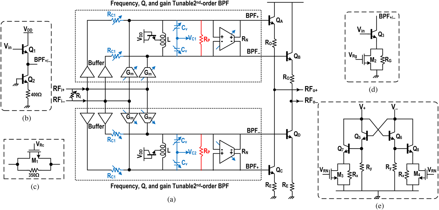
Fig. 4. (a) Schematics diagram of the proposed filter using two 2nd-order BPFs with independent tuning, (b) the buffer cell, (c) the resistance R C1 implementation, (d) the variable Gm cell, and (e) a linearized variable negative resistance R N implementation.
2nd-order BPF tuning
The LC-tanks are driven by a buffer and a transconductor as shown in Fig. 4(a) for voltage and current mode driving, respectively. Since the LC-tanks are driven as well as loaded by active components, no coupling exists between the two resonators, contrary to the case of traditional all-passive ladder and coupled resonator filter structures. Hence, the two LC-tanks can be independently controlled in terms of Q and center frequency tuning. The input buffer, realized by Q 1,2 (Fig. 4(b)), drives the LC-tank in voltage mode. The variable resistor R C consists of an nMOS M1 and a resistor (Fig. 4(c)) which is used to reduce the Q to as low as 4. A variable transconductance G m, realized by Q 3 together with variable resistance R G and M 2 in parallel (Fig. 4(d)) is used to drive the tank in current mode in order to control the gain of the LC-tank. This enables control of the trade-off between noise and linearity. The LC-tank losses R P are compensated by a Darlington-type negative resistance R N as shown in Figure 4(e). This consists of a fixed negative 1/G m realized by Q 5,6 and R Y and a variable negative 1/Gm realized using nMOS M 3,4 and resistance R X. The Q can be increased to more than 100 by controlling the negative resistance using M 3,4. This control also helps in keeping each BPF path stable.
The proposed dual-band band-pass filter, Fig. 4, is implemented in IBM 0.13 µm SiGe BiCMOS process with f T/f max = 180/220 GHz. The fabricated chip photograph is shown in Fig. 5. Great efforts were made to achieve highly symmetric layout for differential matching. The core size of the filter, excluding pads, occupies 0.53 × 0.7 mm2. The total chip area is 1.05 × 0.95 mm2.
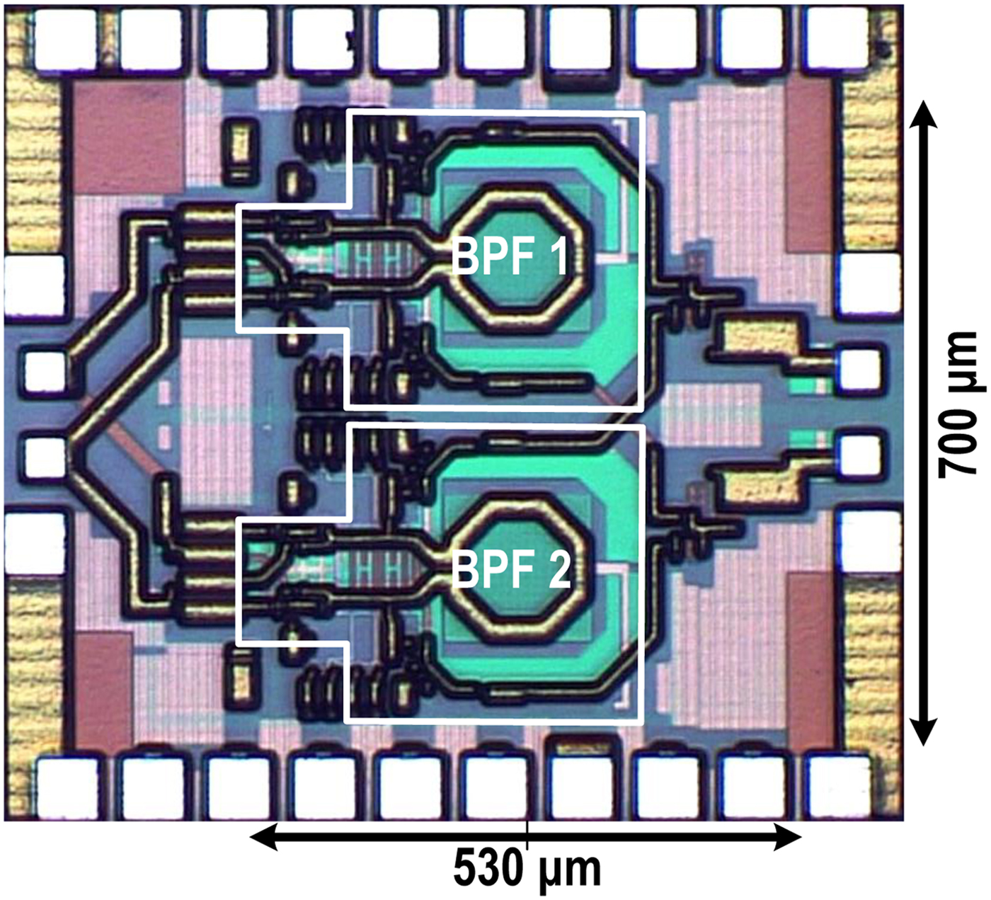
Fig. 5. IBM SiGe 130 nm chip micrograph with core area of 0.7 × 0.53 mm2.
2nd-order BPF Q and stability
On-chip spiral inductors typically have low Q due to the sheet resistance of the inductor metal traces, substrate losses, and the skin effect; these loses can be modeled as a series resistance which must subsequently be mitigated using Q-enhancement. The 2nd-order LC BPF consists of one parallel resonator or tank, which provides two-negative frequency poles. For a lossy on-chip inductor the effective tank Q is that of the inductor with loss RS at the resonance frequency of the tank: 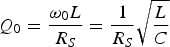 $Q_0= {\omega _0L \over R_S}= {1 \over R_S}\sqrt { {L \over C}}$. Then the equivalent parallel inductor L P and loss R P can be written as
 $$L_P= \Big ({1+Q_0^2 \over Q_0^2} \Big)L_S \; , \;\; R_P=(1+Q_0^2)R_S\approx {\omega_0^2L^2 \over R_S} .$$
A negative resistance R N = −1/G m, to cancel the equivalent parallel loss R P, can be implemented using a transconductor with positive feedback as shown in Fig. 4(e). The equivalent parallel resistance R EQ and the enhanced quality factor Q EN can be expresses as
 $$R_{EQ}= R_P \mid\mid \Big( - {1 \over G_m} \Big)=\displaystyle{R_P \over 1-G_mR_P},$$
 $${\rm and} \quad Q_{EQ}= {R_{EQ} \over \omega_0L_P} = {Q_0 \over 1-G_mR_P}.$$
The Q can be made very high when G mR P → 1. However, the −G m needs to be precisely controlled to avoid oscillation which happens when the equivalent resistance R EQ becomes negative. i.e.G mR P ≥ 1.
Fig. 6(a) shows the Q of the LC-tank before compensation and the total tank Q with a load resistance R C = 350Ω. The inductor Q, based on electromagnetic simulations, varies from 13~18 for frequencies 8~15 GHz whereas the varactor Q varies from 30~115. The resultant LC-tank Q with a load resistance R C = 350Ω is in the range of 9~10 including all parasitic effects from interconnects. With compensation by the negative resistance R N for both tanks, the Q can be increased to 100 or more. Fig. 6(b) shows the post-layout stability simulations of the proposed filter as well as the measured stability factor from S-parameters. The simulation results show that for a Q of 100 for both bands, the stability parameters K¿1 and B1¿0 are satisfied by a large margin guaranteeing that the filter is unconditionally stable over large frequency range. The measured stability parameters are also plotted for Q = 67 from 1 to 22 GHz showing unconditional stability similar to simulations.
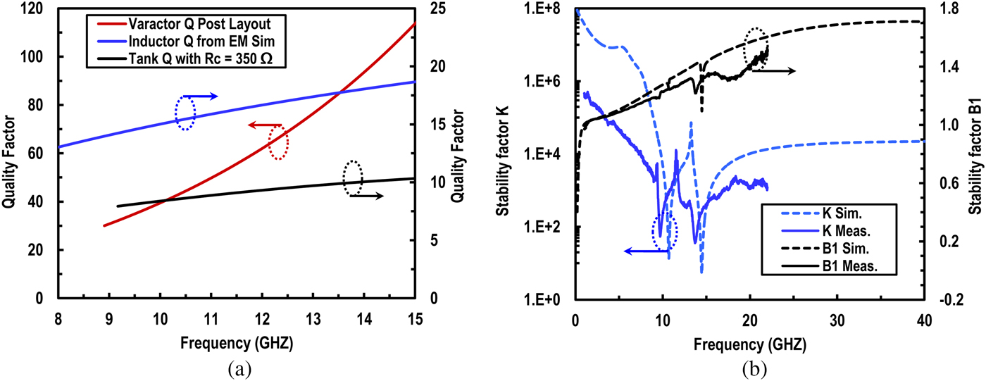
Fig. 6. (a) Post layout simulated Q of the LC-tank components and (b) simulated stability factors when Q is increased to 100 using negative gm and measured stability factors for Q = 67.
Measurement results
To verify the proposed tunable dual-band filter approach, the fabricated chip was measured using GSSG probes with differential SOLT calibration. To interface with single-ended 50 Ω equipment, 180° hybrid couplers were used for differential to single-ended conversion. The measured dual-band filter response is plotted in Fig. 7(a) which shows normalized S 21 plots for different Qs, ranging from 20 to 67. The Q tuning is independent and continuous by controlling each tank's R C and R N (Fig. 4(a)) though only discrete Q tuning steps are shown for clarity. The dual-bands are tuned at 9.7 and 13.9 GHz. With this band-separation, the attenuation is more than 22 dB for BW of 200 MHz each. Due to subtraction, the OOB attenuation on the lower side is > 50 dB below 4 GHz, and, more significantly, > 48 dB on the higher side of the filter at 20 GHz and above. The roll off continues on the lower and upper side frequencies beyond the plot limits. The bands can be tuned independently up and down in frequency using varactor control, while Fig. 7(b) shows the band tuning across the frequency by tuning the lower BPF.
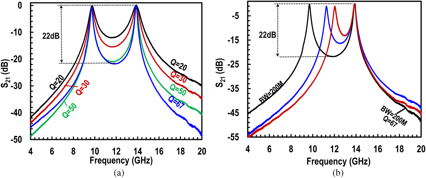
Fig. 7. (a) Measured filter response at 9.7 and 13.9 GHz with Q tuning from 20 to 50 and (b) measured center frequency tuning.
The S 11 and S 22 measurements are shown in Fig. 8(a) for the filter tuned at 9.7 and 13.9 GHz. each with Q of 50. The output matching is very good with S 22 < −14 dB. The S 11 is −10.2 and −8.8 dB at 9.7 and 13.9 GHz, respectively. The group delay measurement plots are shown in Fig. 8(b) for Qs of 20 and 50. The total group delay is around 0.8 ns for Q = 20 and 1.9 ns for Q = 50. The noise figure (NF) and input P −1dB are plotted in Fig. 9(a). The NF is measured for both input matched and high impedance case using R i in Fig. 4(a). The normalized dynamic range (DR), the ratio of input P −1dB to the 1-Hz BW input referred noise, for the input matched case is plotted in Fig. 9(b). The normalized DR varies from 164.6 ~ 154.5 for the lower band, and 160~152 for the upper band for Q = 20 ~ 50 at the expense of 115-130 mW DC power. The measured input P −1dB for Q = 20 ~ 50 is 3~-3.6 dBm and -1~-6 dBm for lower and upper bands, respectively. The NF can be reduced by increasing the gain from the variable transconductance amplifier G m in Fig. 4(a).
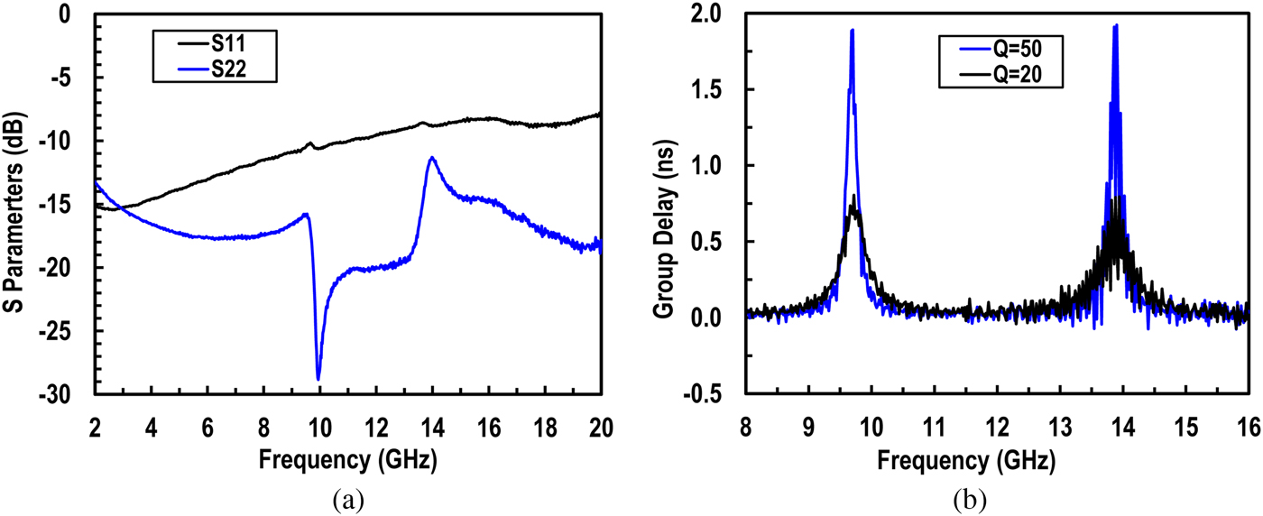
Fig. 8. Measured (a) S 11 and S 22 and (b) group delay for Q of 20 and 50.
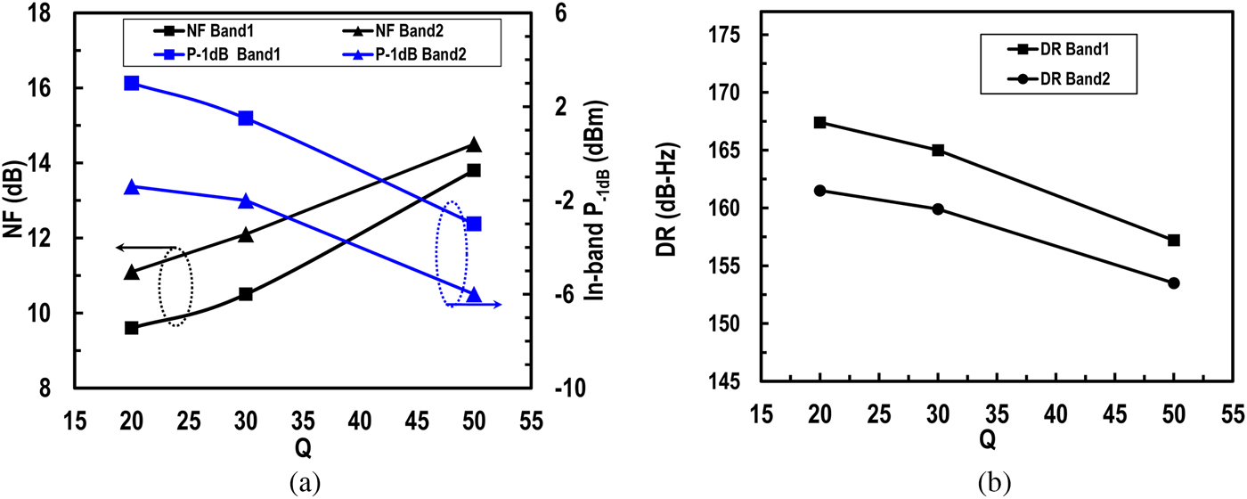
Fig. 9. Measured (a) in-band input P −1dB and noise figure (NF) versus Q and (b) normalized dynamic range.
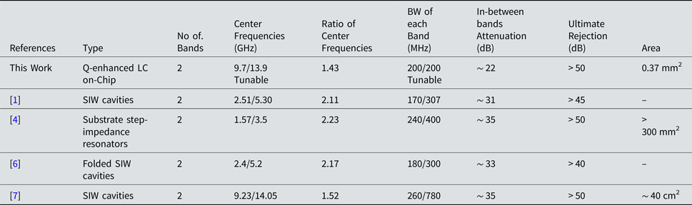
Table 1 shows the performance summary and comparison with state of the art on-chip dual-band filters. The proposed Q-enhanced dual-band filtering is advantageous at microwave frequencies with higher OOB attenuation, independent dual-band tuning, and better DR performance compared with prior integrated N-path filters implementation. Additionally the proposed dual-band filter performance is also compared with off-chip filters in Table 2. The off-chip filters are generally higher-order than this work's 2nd dual-bands. It is also worth mentioning that most of the off-chip filters have dual-band center frequency ratios of more than 2. Apart from small area and flexible tunability, the proposed filter, if designed for frequency ratios > 2, can achieve in-between bands attenuation, as shown in Fig. 2(b), similar to off-chip filters in Table 2.
Table 1. Performance comparison with on-chip filters

aCalculated from 174 + IP−1dB −NF.
b Including CLK generator power.
c Calculated from IIP3 −9.6 dB.
d At 9.7 GHz for Q = 20 ~ 50.
e Insertion loss+0.9 dB (theoretical minimum NF for 4-pth filter [Reference Cook, Berny, Molnar, Lanzisera and Pister14]).
Table 2. Performance comparison with off-chip filters
Conclusion
This paper demonstrated an integrated Q-enhanced dual-band filtering solution at X- and Ku-band microwave frequencies using 0.13 µm SiGe BiCMOS. The concept of dual-band independent tuning operation can be extended to wide range of operating frequencies by appropriately designing the tanks. The filter DR is 164.6–154.5 dB and 160–152 dB at the demonstrated lower (9.7 GHz) and upper (13.9 GHz) bands, respectively. The dual-band filtering approach using the subtraction method has the advantage of increased OOB attenuation on the lower and upper sides of the two passband responses. Future work includes integration of a selection mechanism using switches to provide both subtraction and addition modes on demand depending on system or operational requirements.
Acknowledgments
This work was partially supported by BAE Systems MICS Industry Affiliates Program membership and the Virginia Space Grant graduate fellowship. The silicon chip fabrication was supported by DARPA.
 Farooq Amin received his B.S. degree in computer engineering from COMSATS IIT, Pakistan, in 2005. He received his M.S. degree in electrical engineering with specialization in system-on-chip from Linköping University, Linköping, Sweden in 2009 and the Ph.D. degree in electrical engineering from Virginia Polytechnic Institute and State University, Blacksburg, VA, USA in 2017.
From 2011 to 2013, he was with the CPU design group at Intel Corp. Hillsboro, OR, USA as a Design Engineer working on Intel Hasewell and Broadwell family of microprocessors design. He is currently working for Northrop Grumman Corp. USA as a RFIC Design Engineer. His research interests include RF and mm-wave circuits, analog X-ray read-out circuits and systems, and low-power high speed custom datapath design.
Dr. Amin was the recipient of the IEEE MTT-S International Microwave Symposium Best Student Paper Award (First Place) in 2016. He is also the recipient of Virginia Space Grant Consortium (VSGC) Graduate Fellowship for the years 2015–2017.
 Sanjay Raman was born in Nottingham, U.K., on April 25, 1966. He received the B.S. degree (with highest honor) from the Georgia Institute of Technology, Atlanta, in 1987, and the M.S. and Ph.D. degrees from The University of Michigan at Ann Arbor, in 1993 and 1998, respectively, all in electrical engineering. From 1987 to 1992, he was a Nuclear Trained Submarine Officer with the US Navy. In January 1998, he joined the faculty of the Bradley Department of Electrical and Computer Engineering, Virginia Polytechnic Institute and State University, Blacksburg, where he is currently a Professor. He is also currently serving as Associate Vice President, Virginia Tech National Capital Region, where he is responsible for planning and executing region-wide initiatives to enhance the university's research, education, and outreach missions. He is also a founding member of the VT Multifunctional Integrated Circuits and Systems (MICS) research group. His research interests include RF/microwave/millimeter-wave integrated circuits and antennas, high-speed/mixed-signal ICs, interconnects and packaging, RF microelectromechanical/nanoelectromechanical (MEMS/NEMS) devices, and integrated wireless communications and sensor microsystems.
From 2007 to 2013 he served as a Program Manager with the Microsystems Technology Office, Defense Advanced Research Projects Agency (DARPA), Arlington, VA, responsible for major R&D programs in the areas of adaptive RF/mixed-signal integrated circuits, RF MEMS, and 3D/heterogeneous integration technologies.
Dr. Raman has served as an associate editor for the IEEE TRANSACTIONS ON MICROWAVE THEORY AND TECHNIQUES, and on the Technical Program Committee of the IEEE Radio Frequency Integrated Circuits Symposium. He served as Technical Program Co-Chair for the 2014 International Microwave Symposium. He is an Elected Member of the IEEE Microwave Theory and Techniques Society (MTT-S) Administrative Committee.
He was the recipient of the 2007 Virginia Tech College of Engineering Faculty Fellow, the 2000 Presidential Early Career Award for Scientists and Engineers (PECASE) (1999 NSF CAREER Award), the Virginia Tech College of Engineering Outstanding New Assistant Professor Award (2000), and a 1996–1997 Armed Forces Communications and Electronics Association (AFCEA) Postgraduate Fellowship. In 2013 he was awarded the Secretary of Defense Medal for Exceptional Public Service for his service at DARPA.
 Kwang-Jin Koh received his Ph.D. degree in electrical and computer engineering from the University of California, San Diego in 2008. For his doctoral study, Dr. Koh developed X-band and Q-band silicon phased arrays which were reported to the US DoD by the DARPA as one of the agency's major achievements in 2007–2008 and successfully found their ways into the active protection systems of the US aerospace and defense companies.
After several years stint in the semiconductor industry as an engineering researcher at the Electronics and Telecommunications Research Institute (ETRI, Korea) from 2000 to 2004, as a senior engineer at Intel Corp. from 2008 to 2010, and as a senior staff scientist at Broadcom Corp. from 2010 to 2011, he joined in the Virginia Tech ECE Department as an assistant professor and started teaching from the 2012 Spring semester. Dr. Koh's research interests include low-power and power-efficient integrated circuits and systems up to millimeter-wave frequencies.
Dr. Koh and his students received the first place best student paper award in the 2016 IEEE International Microwave Symposium (IMS) and the second place best student paper award in the 2015 IMS. Dr. Koh was also nominated for the R.W.P. King best paper award from the IEEE Antenna and Propagation Society in 2015. Dr. Koh was the recipient of a best paper award of the IEEE Solid-State Circuits and Electron Device Societies, Seoul Chapter in 2002. He and his Ph.D. student also received the 2015–2017 NASA Virginia Space Grant Consortium STEM research fellowship. Dr. Koh received the 2014 Outstanding Assistant Professor Award and the 2012 Junior Faculty Research Award from the College of Engineering, Virginia Tech, and the 2010 Team of the Year Award from Teledyne Technology Inc. (formerly, Teledyne Scientific Corp.). Dr. Koh has been serving as a technical program committee member of the IEEE Bipolar/BiCMOS Circuits and Technology Meeting and IEEE Custom Integrated Circuits Conference.


