


Introduction
InP HBT technology is increasingly being exploited for integrated circuits operating at higher millimeter-wave and THz frequencies. Compared with competing silicon-based technologies, InP HBT technology leads to higher f max, and higher breakdown voltage for a given technology node. InP HBTs in a 0.25 μm technology node have achieved f max > 1 THz [Reference Urteaga1] and circuits operating at several hundreds of GHz have been demonstrated [Reference Eriksson2, Reference Hacker3].
It is interesting to note that the modeling and RF characterization of these devices are typically based on measurements below W-band. The reason for this is that the influence from probe-to-probe coupling, multi-mode propagation, substrate modes, and radiation losses corrupt the measured transistor data [Reference Schmuckle4]. It remains therefore questionable whether models extracted from measurements below W-band are of sufficient accuracy for circuit design at higher millimeter-wave and THz frequencies. In a recent publication [Reference Li and Zhang5], the first verification of an InP HBT small-signal model up to H-band (220–325 GHz) was reported. The parasitic parameters were extracted from three-dimensional electromagnetic (3D EM) simulations of several test structures and subsequently de-embedded from the transistor measurements to reach the active part of the device. A similar approach has also previously been proposed for millimeter-wave FET modeling [Reference Cidronali6] and shown to provide reasonable accurate small-signal prediction up to 110 GHz.
This paper reports on an EM simulation assisted parameter extraction technique applied to a down-scaled InP HBT in a transferred-substrate technology. The paper provides an expansion of the work described by the authors in [Reference Johansen7]. Our approach differs from that of [Reference Li and Zhang5] in that it relies only on the EM simulation of two structures, a full short and a full open. The distribution of the external parasitic elements necessary to fit EM simulated data up to 325 GHz is determined from equivalent circuit modeling. Properly de-embedding of the parasitic elements, though of small values, are found to have a large influence on the extraction of the remaining parameters associated with the active device structure itself. This applies even if the extraction is restricted to frequencies well below W-band. The proposed EM simulation assisted parameter extraction is shown to lead to more reliable extraction and is proven to extend the validity of the model to frequencies higher than those typically employed for extraction. The paper is organized as follows. In section 2, the test structure layout for the device-under-test is described as is the multi-line Through-Reflect-Line (TRL) calibration procedure used. Section 3 deals with the EM simulation-based modeling of the parasitic network embedding the device-under-test. Aspects of the parameter extraction associated with the active device part is described in section 4. The model verification against experimental results is given in section 5. Finally, section 6 concludes the paper.
Test-structure layout and calibration
The InP HBT were fabricated in a transferred-substrate TMIC (THz Monolithically Integrate Circuit) technology at the Ferdinand-Braun-Institute (FBH). Compared with the base-line device having an 0.8 μm technology node [Reference Weimann8], the experimental device here has been downscaled to an 0.5 μm technology node and its device layout has been compacted. The transferred-substrate process start out with a conventional emitter-up InP/InGaAs/InP double-heterostructure grown by solid-source molecular beam epitaxy on a semi-insulating 3′ InP substrate. The structure is planarized with BCB, which also serves as the adhesive in wafer-bonding the half-processed InP HBT wafer to the 3′ ceramic AlN host substrate. Post wafer bonding, the InP substrate was removed wet-chemically, followed by collector processing and addition of G1 and G2 first and second-level interconnects. An 2.5 μm thick electroplated interconnect layer, Gd, serves as RF ground. Contact holes V1 and V2 provide the vertical connections between Gd, G1, and G2, and serve to contact the B1 base metal tab (see Fig. 1). Figure 2 shows a microphotograph of the on-wafer test structure for the 0.5 × 6 μm2 InP HBT in common-emitter configuration. The reference planes for model extraction is as shown in Fig. 2. For versatile circuit design the transfer-substrate InP HBTs also come in three-terminal versions.
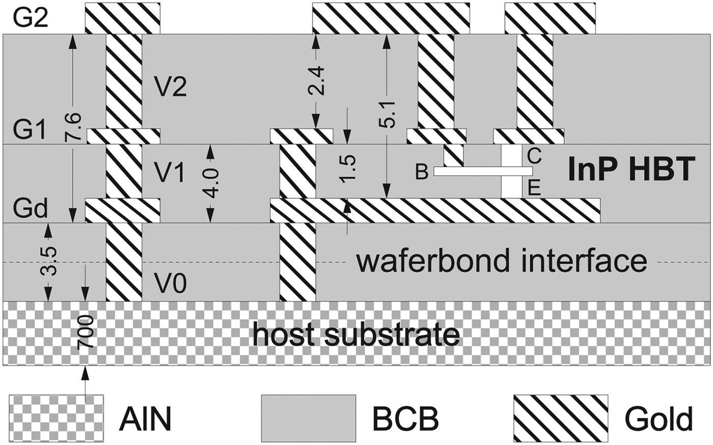
Fig. 1. Vertical cross-section of transferred-substrate InP HBT TMIC technology (all measures are given in μm).
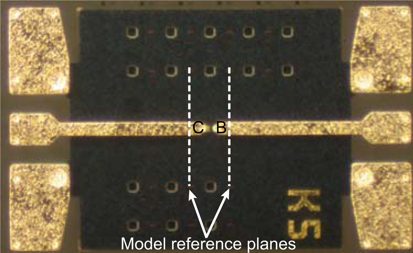
Fig. 2. Microphotograph of on-wafer test structure for 0.5 × 6 μm2 InP HBT showing reference planes for model extraction.
A multi-line TRL calibration procedure using on-wafer standards is used to shift the reference planes to the middle of the thin-film microstrip (TFMS) through line. The effective line lengths are 452, 1282, 1982, and 2882 μm covering a frequency range from ~4 to 220 GHz. Both an open and a short symmetrical reflect structures are used for increased accuracy. The multi-line TRL calibration procedure only provides information about the complex propagation constant γ = α + jβ and sets the reference impedance to the characteristic impedance of the line structures [Reference Marks9]. For renormalization of the corrected S-parameters to 50 Ω, the characteristic impedance Z 0 must be known. The characteristic impedance can be found from the capacitance per unit length, C′, if the dielectric loss is negligible. A good estimate for C′ is possible using measurement of a resistor embedded into the same line structure as used for calibration assuming it to have small dielectric loss and low dispersion in C′ [Reference Williams and Marks10]. Under this condition C′ can be estimated as
 $$C^{\prime}\approx {\displaystyle{\gamma} \over {\,j\omega R_{res, dc}}}{\displaystyle{{1 + \Gamma_{res}} \over {1- \Gamma_{res}}}}, $$
where R res,dc is the DC value of the resistor and Γres is the reflection coefficient of the resistor using the multi-line TRL corrected resistor measurement. The characteristic impedance is estimated as Z 0 ≈ γ/jωC′. The corrected S-parameters using the renormalized multi-line TRL approach compares well with our former approach based on off-wafer LRM+ calibration followed by de-embedding of pads and access transmission lines [Reference Johansen11]. The main advantage of using the multi-line TRL calibration procedure is its expected better accuracy at higher frequencies [Reference Derrier, Rumiantsev and Celi12].
Parasitic modeling
Parasitic model structure
A detailed cross-sectional view of the transferred-substrate InP HBT structure is shown in Fig. 3. From the device structure in Fig. 3 a detailed parasitic network, as shown in Fig. 4, can be identified. The parasitic network includes coupling capacitances between metal layers, C g2−g2, C g2(g1)−gd, C g1−g1, and C g1−b1, frequency-dependent inductances of vias and electrodes, L v2b(f), L v2k(f), L v1b(f), L b1(f), L k(f), and L e(f), and frequency-dependent resistances, R v2b(f), R v2k(f), and R b1(f). The base and collector of the device are connected to the surrounding network by short TFMS lines. The shown parasitic network, however, is expected to be overcomplex even for modeling up to THz frequencies. In the following, the parameters of the parasitic network will be extracted from EM simulations and the distribution necessary to fit simulation results up to 325 GHz will be found from equivalent circuit modeling.

Fig. 3. Detailed cross-section of InP HBT in microstrip test frame. The shaded areas represent the active transistor layers.

Fig. 4. Active device embedded in detailed parasitic model structure.
EM simulation of parasitic network
EM simulation of the parasitic network is performed with the InP HBT active device part, shown as the shaded area in Fig. 3, either open-circuited or short-circuited. In the open test structure, the shaded areas are replaced by BCB while these areas consist of gold in the short structure.
The 3D finite-element-method simulator Ansys HFSS is used. The structures are meshed at 325 GHz using an initial wavelength-based mesh setting of ≤0.05λ. For accurate simulation of the skin-effect, fields are solved inside all conductors and an initial internal mesh seeding is employed. The structures are excited with lumped ports (P1 and P2) between the G2 and Gd metal layers. For highest accuracy when simulating small-sized on-wafer structures, the port excitation must be calibrated. This is accomplished by applying the L-2L calibration methodology for EM simulation accuracy enhancement as described in [Reference Johansen13]. In this way, the parasitic port inductance and port capacitance is estimated to be ~0.9 pH and ~0.38 fF, respectively, and fairly constant with frequency. These port parasitics are calibrated from all shown EM simulation results.
Effective capacitances
 $$C_{\,pb} = {C_{g2 - gd}} + {C_{g1 - gd}} + {C_{b1 - gd}} = {\displaystyle{1} \over {2\pi f}} \Im (Y_{22} + Y_{12}),$$
 $$C_{q} = C_{g2 - g2} + C_{g1 - g1} + C_{g1 - b1} = {\displaystyle{1} \over {2\pi f}} \Im (-Y_{12}),$$
 $$C_{\,pc} = C_{g2 - gd}+C_{g1 - gd} = {\displaystyle{1} \over {2\pi f}} \Im(Y_{11} + Y_{12})$$
can be extracted from the EM simulation result for the full open structure by assuming a pi-type equivalent circuit. The extracted effective capacitances are shown in Fig. 5(a) as the curves with solid lines. It is observed that the dispersion in their extracted values over frequency is limited. Similarly, effective inductances
 $$L_{\,pb}(\,f) = L_{v2b} + L_{v1b} + L_{b1} = {\displaystyle{1} \over {2\pi f}} \Im (Z_{22} - Z_{12}),$$
 $$L_{\,pe}(\,f) = {\displaystyle{1} \over {2\pi f}} \Im (Z_{12}),$$
 $$L_{\,pc}(\,f) = L_{v2k} + L_{k} = {\displaystyle{1} \over {2\pi f}} \Im (Z_{11} - Z_{12}),$$
and effective resistances
 $$R_{\,pb}(\,f) = R_{v2b} + R_{b1} = {\frak R}(Z_{22} - Z_{12}),$$
 $$R_{\,pe}(\,f) = {\frak R}(Z_{12}),$$
 $$R_{\,pc}(\,f) = R_{v2k} = {\frak R}(Z_{11} - Z_{12})$$
can be extracted from the EM simulation result for the full short structure by assuming a T-type equivalent circuit. The extracted effective inductances and resistances are shown in Figs 5(b) and 5(c), respectively, again as curves with solid lines. The frequency dispersion in the extracted inductances and resistances are more significant than for the extracted effective capacitances.
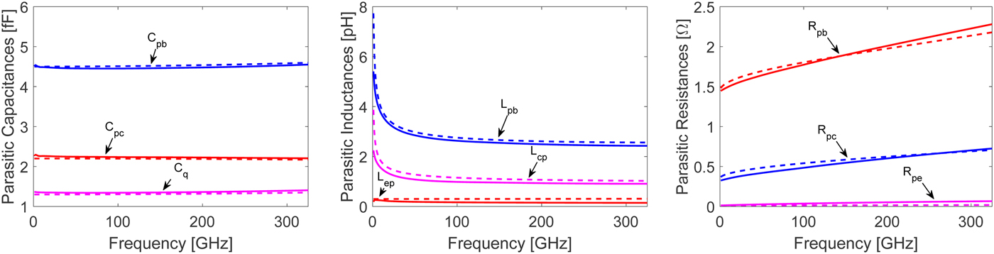
Fig. 5. Extracted (solid lines) and modeled (dashed lines) for (a) parasitic capacitances for full open, (b) parasitic inductances for full short, and (c) parasitic resistances versus frequency for full short.
Equivalent circuit modeling of parasitic network
The dispersion over frequency in the extracted parasitic network parameters are caused by distribution along the device access structure and skin-effect due to field penetration into the conductors. It is found that the initial strong frequency dependence of the extracted inductances is consistent with the skin-effect causing the observed increase in the extracted resistances. The parasitic resistances can thus be described with equations of the form
 $$R_{\,p}(\,f) = R_{\,p}(\,f = 0) + R_{\,p,ac}\sqrt{\,f},$$
where R p(f = 0) is the DC resistance and R p,ac is the ac resistance normalized to the square-root of frequency for describing the skin-effect. It is well known that the skin-effect gives rise to a reactance of equal magnitude to the AC resistance. Therefore, for consistency the parasitic inductances must be described by equations of the form
 $$L_{\,p}(\,f) = L_{\,p}(\,f\rightarrow \infty) + R_{\,p,ac}/(2\pi \sqrt{\,f}),$$
where L p(f → ∞) is the assumed frequency-independent inductance reached once the EM field inside the conductors has vanished. The above formulation gives the well-known  $\sqrt {f}$-dependent increase in the ac resistance value and $1/\sqrt {f}$-dependent decrease for the inductance value. At very low frequencies the inductance should converge to its static value but this is not implemented in the model for simplicity. Instead, the model implements a frequency-dependent impedance as
 $$\eqalign{Z_{\,p}(\,f) = R_{\,p}(\,f = 0) & + j2\pi f L_p(\,f\rightarrow \infty) \cr & + R_{\,p,ac}\sqrt{\,f}(1 + j).}$$
In this way, the singularity in (12) as f → 0 is avoided. The parasitic capacitances can be assumed to be frequency independent. The dispersion in the values for the extracted effective capacitances, though weak, is an indication of distribution along the device access structure. The identification of the parasitic model structure necessary to fit theelctromagnetic (EM) simulation results up to 325 GHz follows a straightforward procedure. At first, the total capacitances in the parasitic model structure are determined from the effective capacitance values extracted at low frequency. The parasitic inductances, L p(f → ∞), are determined from the effective inductances extracted at the highest simulation frequency. At the same time the DC resistances, R p(f = 0), are determined from the effective resistances extracted at the lowest frequency. The ac resistances normalized to the square-root of frequency, R p,ac, are determined by simultaneously fitting of the effective inductances and effective resistances extracted over frequency. The distribution of the total capacitances along the device access structure is found to have a negligible effect on the dispersion observed in the effective inductances and effective resistances. On the other hand, the distribution of capacitances is found to have an influence on the dispersion of the effective capacitances for the open structure. Due to the weak dispersion, simple distribution factors X pb, X q and X pc are sufficient to fit the effective capacitances extracted from the open structure. The identified parasitic model structure is shown in Fig. 6. Though some physical significance of the equivalent circuit elements is lost compared with the detailed parasitic model structure in Fig. 4 it is sufficient to model the parasitic network structure, at least up to 325 GHz. The curves with dashed lines in Figs 5(a)–5(c) showthe excellent fitting all the way up to 325 GHz using this equivalent circuit modeling approach. Table 1 provides a summary of the parasitic model parameters determined fromthree-dimensional (3D) EM simulations. For comparison the external base and collector parasitic capacitance estimated from cut-off mode measurements are shown in parenthesis. There is a good agreement between these values and those found from our EM simulation assisted extraction procedure. The model parameters representing the extrinsic emitter resistance, R pe(f) are negligible for a transferred-substrate InP HBT in common-emitter configuration but gain significance for a three-terminal InP HBT.
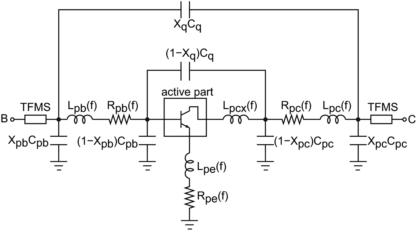
Fig. 6. Active device embedded in parasitic model structure.
Table 1. Parasitic model parameters (elements in parenthesis are extracted from cut-off mode measurements)

Parameter extraction for active model
The measurements for parameter extraction was performed on-wafer using 100 μm pitch GSG Picoprobes from GGB Industries and a Keysight PNA with OML frequency extenders to 110 GHz. In the proposed EM simulated assisted parameter extraction approach, the parasitic network elements found from 3D EM simulations are de-embedded from the multi-line TRL corrected transistor measurements. Following this de-embedding the equivalent circuit model in Fig. 7 should be sufficient to describe the active part of the InP HBT. Conventional extraction techniques are not able to provide the same degree of details for the parasitic network as that obtained by our EM simulation to 325 GHz. In the approach reported in [Reference Johansen11], the collector-emitter overlap capacitance, C pc, is determined from cut-off mode measurements and de-embedded from all active device measurements. Any remaining base-emitter and base-collector overlap capacitances are absorbed into the base-emitter capacitance, C be, and extrinsic base-collector capacitance, C bcx, respectively. Residual terminal inductances not removed by de-embedding are extracted at high frequencies using intrinsic elements extracted at lower frequencies. The EM simulation assisted parameter extraction is proposed to solve the problem with external parasitic element extraction which cannot be extracted with sufficient details using the experiment data.

Fig. 7. Equivalent circuit model for active part of InP HBT.
As described in details in [Reference Johansen11], the parameter extraction technique for the active device part exploits the physical behavior of the base-collector capacitance in InP HBTs
 $$ C_{bc} = C_{bc0} - {\displaystyle{k_1I_c} \over {2}}\left(1-{\displaystyle{I_c} \over {I_{tc}}}\right), $$
where C bc0 is the base-collector capacitance at zero bias current and I c is the collector current. The parameters k 1 and I tc describe electron velocity modulation effects in the collector region. The parameters of (13) is found by fitting extracted values for the base-collector capacitance versus collector current as shown in Fig. 8. The base-collector capacitance is extracted from measured Z-parameters as
 $$C_{bc}\approx {\displaystyle{1} \over {\omega}} \Im \left({\displaystyle{1} \over {Z_{22}} - Z_{21}}\right). $$
The dashed line in Fig. 8 is a plot of (14) using parameters C bc0 = 5.1 fF, k 1 = 0.48 ps/V, and I tc = 13.8 mA. Figure 8 also shows the extracted values for the base-collector capacitance without de-embedding of the parasitic network elements. As shown, an effect of neglecting the parasitic network is that the base-collector capacitance associated with the active device itself will be overestimated and the curvature versus collector current slightly different from the one determined from the de-embedded data. From measured Z-parameters it is possible to define an effective base resistance as
 $$ R_{b,eff}={\frak R}(Z_{11}-Z_{12}). $$
At low injection levels, it is possible to approximate this effective base resistance as
 $$ R_{b,eff}\approx R_{bx}+X_0\left(1-(1-X_0){\displaystyle{I_c} \over {I_p}}\right)R_{bi}, $$
where X 0 is the zero current distribution factor between the intrinsic and total base-collector capacitance and I p = 2X 0C bc0/k 1 is a characteristic current [Reference Johansen11]. The zero current distribution factor can be extracted from cut-off mode measurements in a lower frequency range, here selected from 4 to 14 GHz. It is found that the extracted zero current distribution factor varies from X 0 ≈ 0.6 without de-embedding of the parasitic network to X 0 ≈ 0.32 with de-embedding. From (17) it is seen that the linear extrapolation of R b,eff values plotted versus 1 − (1 − X 0)I c/I p to the collector current I c = I p/(1 − X 0) should give the extrinsic base resistance, R bx. The initial slope of the plot should correspond to X 0R bi and hence gives a way to extract a value of R bi if X 0 is known [Reference Johansen14]. The procedure is illustrated in Fig. 9. The effective base resistance, R b,eff, is averaged over the frequency range from 4 to 65 GHz. The dashed line is a plot of (17) using parameters X 0 = 0.32, I p = 6.8 mA, R bx = 5.8 Ω and R bi = 40.0 Ω. In general, the extracted data at low injection followthe expected trend given by (17). Figure 9 also shows the extracted R b,eff plotted versus 1 − (1 − X 0)I c/I p for the situation without de-embedding of the parasitic network. As observed the extraction method fails in this case as it is not possible to fit an equation of the form given by (17) to the extracted data. The parasitic network elements, though of small value, are thus found to have a surprisingly large influence on the extracted parameter values using the method above. A more detailed analysis reveals that the large influence stems mainly from the parasitic capacitances distributed along the base and collector electrodes which become more significant for the down-scaled devices considered here. The residual inductances are actually of secondary influence for these devices. This is because the parameter extraction method reported in [Reference Johansen11] and later refined in [Reference Johansen14] is largely independent of any external terminal inductances.
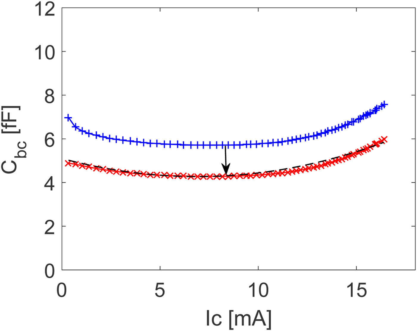
Fig. 8. Extraction with (solid line with crosses) and without (solid line with pluses) parasitic network de-embedding for base-collector capacitance versus collector current. The dashed line is a plot of (12) using parameters C bc0 = 5.1 fF, k 1 = 0.48 ps/V, and I tc = 13.8 mA. The collector-emitter bias voltage is V ce = 1.8 V.
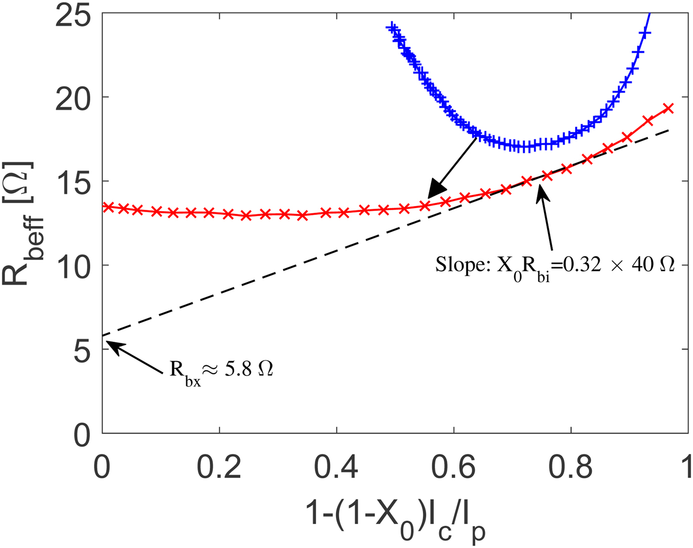
Fig. 9. Extraction with (solid line with crosses) and without (solid line with pluses) parasitic network de-embedding for effective base resistance versus 1 − (1 − X 0)I c/I p. The dashed line is a plot of (14) using parameters X 0 = 0.32, I p = 6.8 mA, R bx = 5.8 Ω and R bi = 40.0 Ω. The collector-emitter bias voltage is V ce = 1.8 V.
As a further verification of the EM simulation assisted parameter extraction approach, a well-established method to extract the intrinsic base resistance is investigated [Reference Suh15]. For this purpose a distributed base impedance
 $$ Z_{b,dist} = {\displaystyle{Z_{11}(Z_{22}-Z_{12})+Z_{12}(Z_{12}-Z_{21})} \over {Z_{22}-Z_{12}}} $$
is formulated. The asymptotic value at high frequencies for the real part of the distributed base impedance in (18) should correspond to the intrinsic base resistance R bi [Reference Suh15]. In Fig. 10, it is observed that the asymptotic value approaches 42 Ω, very close to the 40 Ω extracted from the method of [Reference Johansen14]. Table 2 provides a summary of the extracted equivalent circuit elements for the active device model in Fig. 7. A few parameters have been tuned following the direct extraction procedure to provide the best possible fit to the measured S-parameter data in the 0.05 to 110 GHz frequency range.
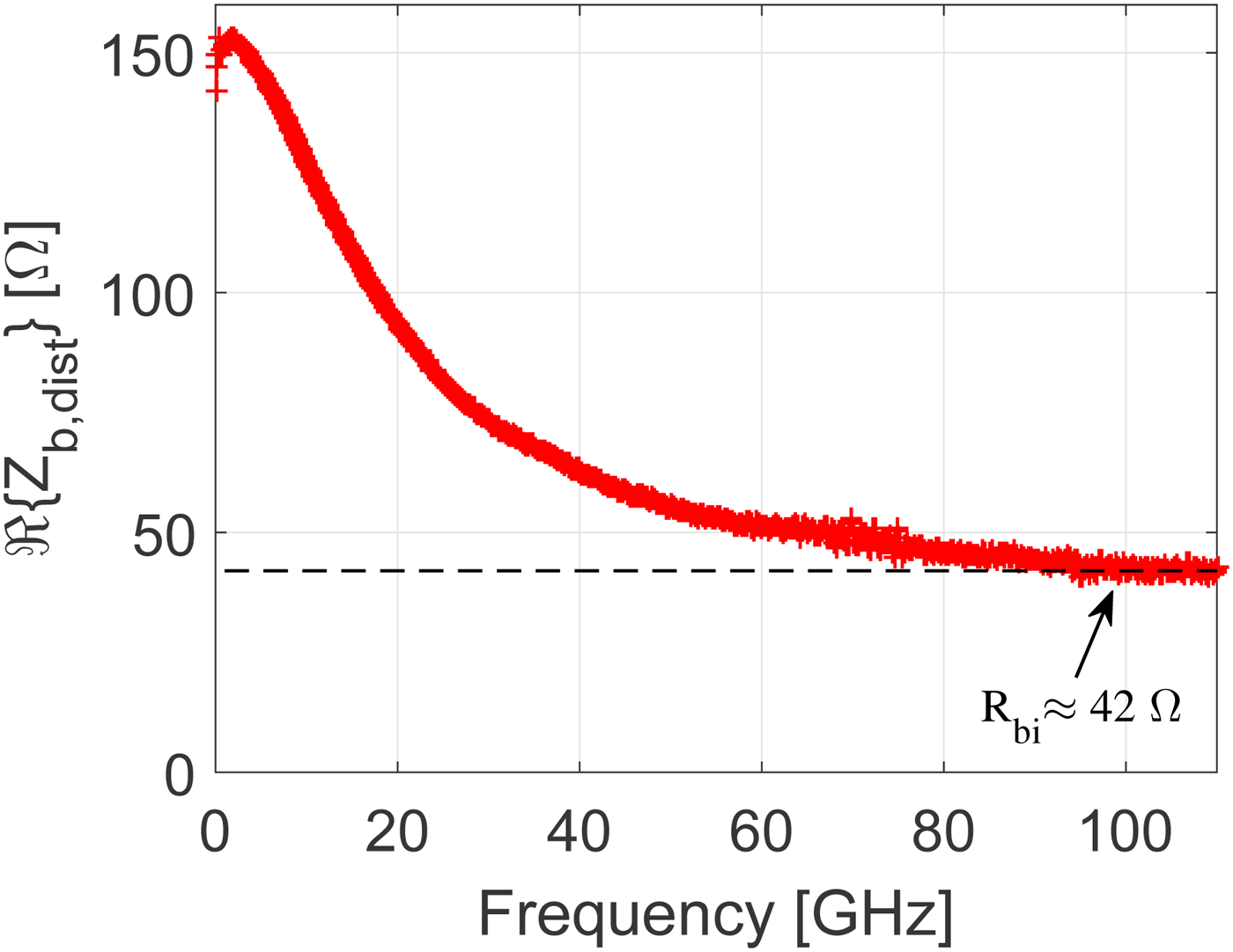
Fig. 10. Real part of distributed base impedance versus frequency. The dashed line indicates the asymptotic value using R bi ≈ 42 Ω. The bias point is V ce = 1.8 V, I c = 8 mA.
Table 2. Extracted equivalent-circuit elements (V ce = 1.8 V, I c = 8 mA)

Model verification
Figure 11 compares the measured S-parameters at two bias points to the small-signal model structure for the active device augmented with the distributed parasitic network as shown in Fig. 6. The bias point of V ce = 1.8 V, I c = 8 mA corresponds to the peak of the extracted f max versus I c characteristic while that of V ce = 1.8 V, I c = 2.9 mA represents low injection. A good agreement between experimental and modeled data is observed in the 50 MHz–110 GHz frequency range for both bias points. There are some slight deviations from expected behavior in the measured S-parameters at the highest frequencies around 110 GHz. These are expected to be caused by the aforementioned complications associated to probe-to-probe coupling, parasitic modes, and radiations in an on-wafer measurement environment. This is confirmed by the small-signal measurements in the frequency range from 140 to 220 GHz (G-band). The trend of the S-parameters in this frequency range is well predicted by the small-signal model. The measurement from 140 to 220 GHz was performed on-wafer using 50 μm pitch GSG Picoprobes from GGB Industries and a ZVA Rohde & Schwarz VNA with G-band frequency extenders. The shown S-parameters have been corrected using the multi-line TRL procedure as described in section 2.
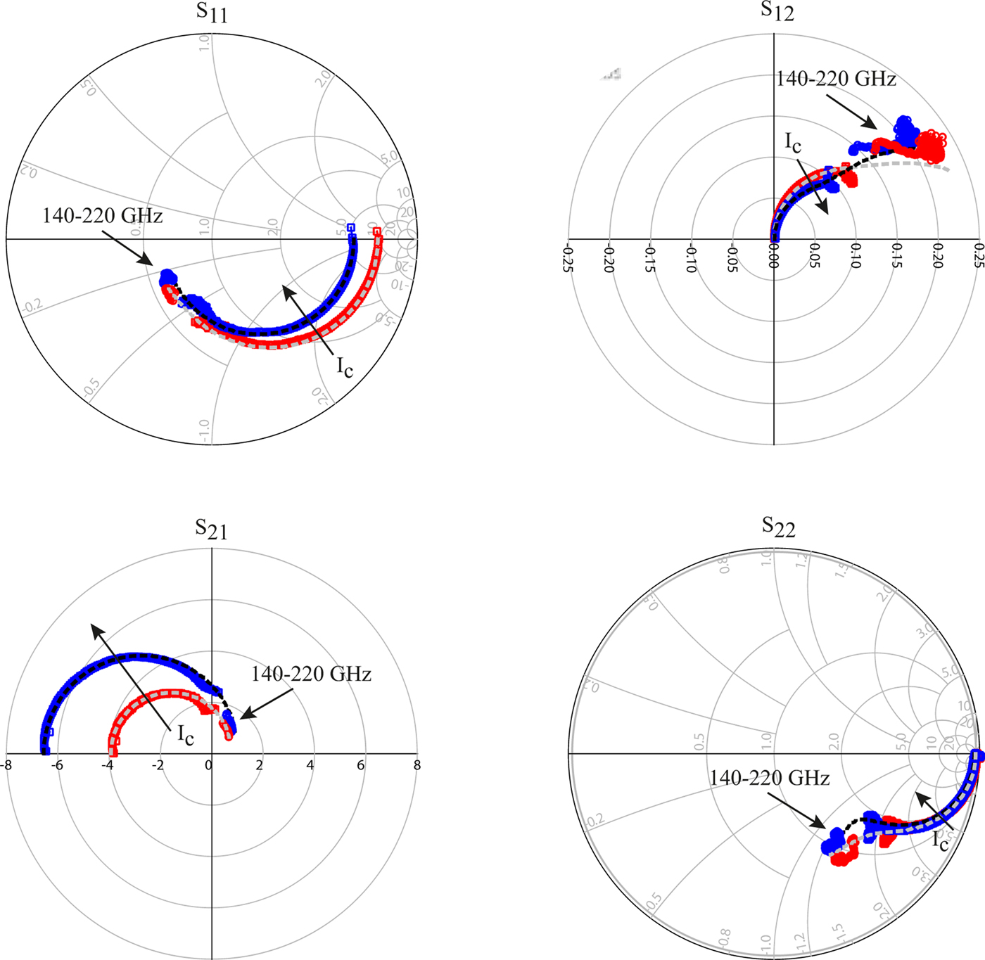
Fig. 11. Comparison of measured (solid lines with symbols) and modeled (dots) S-parameters in the frequency range from 50 MHz to 110 GHz and 140 to 220 GHz. The bias points are V ce = 1.8 V, I c = 2.9 mA, and V ce = 1.8 V, I c = 8.0 mA.
For further experimental verification of the small-signal prediction globally derived quantities should be used. This allows the model validation to take into account the way any discrepancies in the prediction of each individual S-parameter combine within these globally derived quantities [Reference Resca16]. In Fig. 12 the magnitude of the short-circuited current gain, |H 21| is plotted versus frequency. The extrapolated small-signal prediction excellently predicts the |H 21| extracted from the experimental data in the 140 to 220 GHz frequency range. For clarity only the results for V ce = 1.8 V, I c = 8 mA are shown in the following. Another important derived quantity is Mason's gain, U. This quantity is often used to extract the maximum frequency of oscillation, f max, from linear extrapolation assuming a −20 dB/decade slope. It is well known that f max extraction from experimental data can be complicated. Figure 13 illustrates clearly how the extracted Mason's gain is only showing the expected −20 dB/decade slope in a limited frequency range around 30 GHz leading to some ambiguity in the extracted f max value (f max ≈ 400 GHz). Interestingly, Mason's gain extracted from the 140 to 220 GHz data is well predicted by the small-signal model and follows overall a −20 dB/decade slope. This confirms that the unexpected behavior below 110 GHz is caused by the aforementioned complications associated with on-wafer measurements. The high-frequency measurements do not suffer so much from these unwanted effects. This may be related to the more compact setup using the G-band probes for on-wafer measurements. As a final verification, the maximum-available-gain, G mag, or the maximum-stable-gain, G msg, whenever the stability factor K < 1 [Reference Vidkjær17] will be considered. G mag is an important globally derived quantity which is a strong indicator of the achievable performance for a given millimeter-wave and THz circuit. The distribution of the elements of the small-signal model is important to predict the division point in frequency between G msg where the stability factor K is <1 and G mag where K is >1. As is observed in Fig. 14 the small-signal model captures this division point accurately. Again it is observed how the small-signal prediction in the highest frequency range from 140 to 220 GHz confirms the experimental results. There are some discrepancies between measurements and model simulations observed at frequencies below 1 GHz. These discrepancies could be caused by S-parameter data being outside the frequency range set by the lengths of the multi-line TRL calibration line standards.
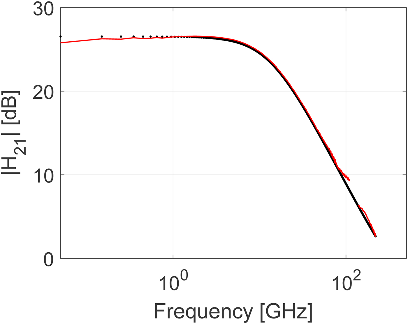
Fig. 12. Comparison of measured (solid lines) and modeled (dots) magnitude of short-circuited current gain, |H21|, versus frequency in the frequency range from 50 MHz to 110 GHz and 140 to 220 GHz. The bias point is V ce = 1.8 V, I c = 8 mA.
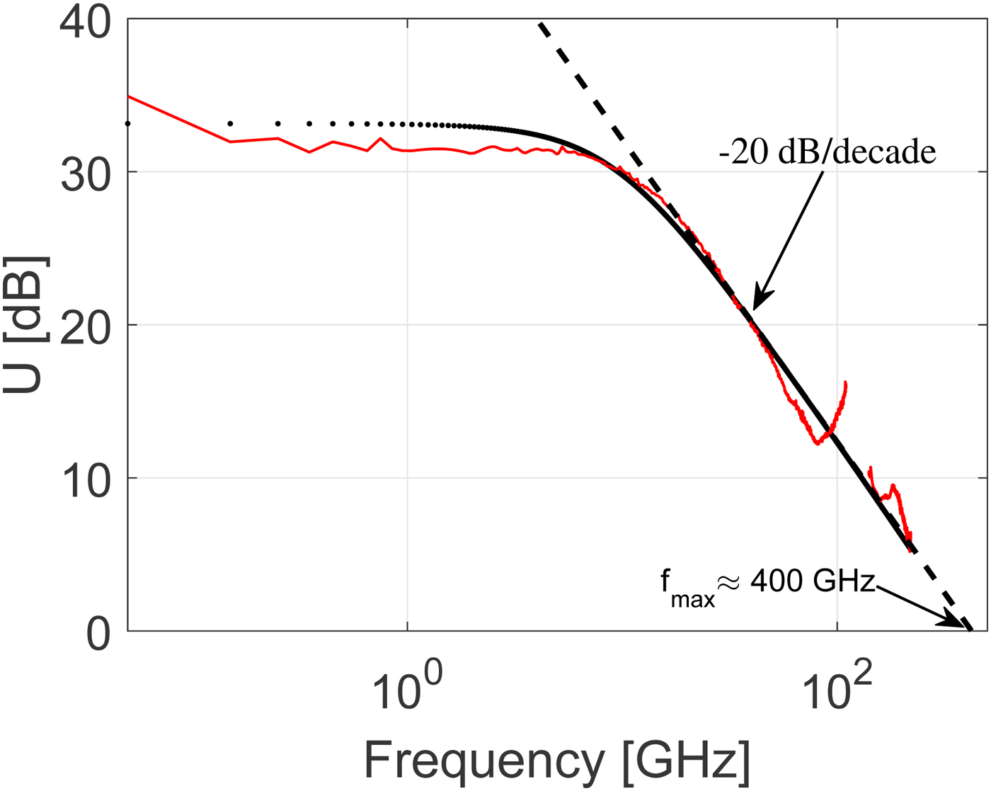
Fig. 13. Comparison of measured (solid lines) and modeled (dots) Mason's gain, U, versus frequency in the frequency range from 50 MHz to 110 GHz and 140 to 220 GHz. The bias point is V ce = 1.8 V, I c = 8 mA.
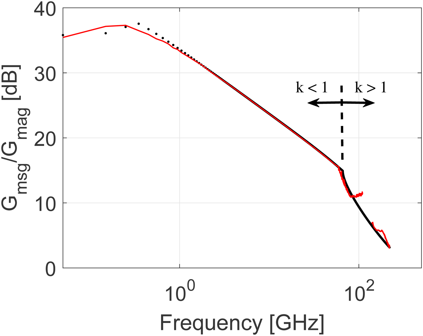
Fig. 14. Comparison of measured (solid lines) and modeled (dots) maximum stable gain/maximum available gain, G msg/G mag, versus frequency in the frequency range from 50 MHz to 110 GHz and 140 to 220 GHz. The bias point is V ce = 1.8 V, I c = 8 mA.
Conclusion
An EM simulation assisted parameter extraction approach has been described. The approach relies on accurate 3D EM simulations of the external parasitic network associated with down-scaled InP HBTs in transferred-substrate technology. De-embedding the parameters of the parasitic network from the multi-line TRL-corrected transistor measurements leads to greater reliability in the extraction of the parameters associated with the active device. The accurate prediction of the S-parameters and derived quantities even in the 140 to 220 GHz frequency range verifies the small-signal model augmented with the parasitic network. The increased distribution of the small-signal model leads to confidence in our modeling approach to even higher millimeter-wave and THz frequencies. Future work will focus on scaling of the approach to smaller devices and experimental verification to higher frequencies.
Acknowledgments
The authors would like to thank Steffen Schulz for measurements.
 Tom K. Johansen received his M.S. and Ph.D. degrees in Electrical Engineering from the Technical University of Denmark, Denmark, in 1999 and 2003, respectively. In 1999, he joined the Electromagnetic Systems Group, DTU Elektro, Technical University of Denmark, Denmark, where he is currently an Associate Professor. From September 2001 to Marts 2002 he was a Visiting scholar at the center for wireless communication, University of San Diego, California, CA. He has spent several external research stays at the Ferdinand Braun Institute (FBH), in Berlin, Germany. His research areas include the modeling of high-frequency solid-state devices, millimeter-wave and sub-millimeter-wave integrated circuit design.
 Ralf Doerner received the Dipl. Ing. degree in Communications Engineering from the Technische Universität Ilmenau, Ilmenau, Germany, in 1990. Since 1989, he has been working on microwave measuring techniques. In 1992, he joined the Ferdinand-Braun-Institut, Leibniz-Institut für Höchstfrequenztechnik, Berlin, Germany. His current research is focused on calibration problems in on-wafer millimeter-wave and sub-millimeter-wave measurements of active and passive devices and circuits. Further research activities include non-linear characterization of microwave power transistors and noise characterization and modeling of microwave devices. He received the 71th ARFTG Best Interactive Forum Paper Award and the 2011 European Microwave Prize.
 Nils G. Weimann received the Diploma degree (with honors) in Physics from the University of Stuttgart, Germany, in 1996, and the Ph.D. degree in Electrical Engineering from Cornell University, Ithaca, NY, USA in 1999. He then joined Bell Laboratories in Murray Hill, NJ, as a Member of Technical Staff, and became a Technical Manager there in 2003. From 2012 on, he was leading the InP Devices Lab at the Ferdinand-Braun-Institute, Leibniz-Institute for High Frequency Electronics in Berlin, Germany. Since 2017, he is the High Frequency Electronic Devices Chair Professor in the Department of Electrical Engineering and Information Technology at the University of Duisburg-Essen, Germany. His research interests include indium phosphide and gallium nitride high-frequency semiconductor components and circuits. He has authored or co-authored more than 120 publications and conference contributions, and he holds 12 patents in the field of high-frequency electronics and integrated optoelectronics.
 Maruf Hossain received his M.Sc. degree in Electronics/Telecommunication from the University of Gavle, Gavle, Sweden in 2008 and Ph.D. degree in Electrical Engineering from Technical University of Berlin, Berlin, Germany in 2016. In 2008, he joined in IHP Microelectronics in the Circuit Design Department, Frankfurt/Oder, Germany. Since 2011, he has been with the Ferdinand-Braun-Institut (FBH), Berlin, Germany. His research interests include the CMOS/BiCMOS, millimeter wave, and THz MMIC circuit design and characterization.
 Viktor Krozer received the Dipl.-Ing. and Dr.-Ing. degree in Electrical Engineering at the Technical University Darmstadt in 1984 and in 1991, respectively. In 1991, he became the senior scientist at the TU Darmstadt working on high-temperature microwave devices and circuits and submillimeter-wave electronics. From 1996 to 2002 Dr. Krozer was professor at the Technical University of Chemnitz, Germany. From 2002 to 2009 Dr. Krozer was Professor at Electromagnetic Systems, DTU Elektro, Technical University of Denmark, and was heading the Microwave Technology Group. Since 2009 Dr. Krozer has been an endowed Oerlikon-Leibniz-Goethe professor for Terahertz Photonics at the Johann Wolfgang Goethe University Frankfurt, Germany and heads the Goethe-Leibniz-Terahertz-Center at the same university. He is also with FBH Berlin, leading the THz components and systems group. His research areas include terahertz electronics, MMIC, non-linear circuit analysis and design, device modelling, and remote-sensing instrumentation.
 Wolfgang Heinrich received the diploma, Ph.D., and habilitation degrees from the Technical University of Darmstadt, Germany. Since 1993, he has been with the Ferdinand-Braun-Institut (FBH) at Berlin, Germany, where he is the Head of the Microwave Department and Deputy Director of the institute. Since 2008, he is also Professor at the Technical University of Berlin. His present research activities focus on MMIC design with emphasis on GaN power amplifiers, mm-wave integrated circuits, and electromagnetic simulation. Professor Heinrich has authored or coauthored more than 350 publications and conference contributions.


