


Introduction
The increasing integration level of modern communication, computer, automotive, and consumer electronics as well as in areas such as system control introduce higher requirements for modern manufacturing processes utilizing the lower industrial, scientific, and medicalfrequency bands, especially at 13.56, 27.12, and 40.68 MHz. These manufacturing processes generate a significant demand for low-loss, fast and highly tunable radio frequency (RF) varactors e.g. for the realization of matching circuits. Currently available technologies are mechanically tuned vacuum capacitors and switchable capacitor banks, utilizing high-power pin diodes. However, the limited tuning speed of the mechanically tunable vacuum capacitors presents a significant drawback, while the switchable capacitor banks only provide discrete capacitance steps. Varactors based on ferroelectric material such as barium strontium titanate (BST) have been under investigation for several years now and show promising results regarding tunability, tuning speed, Q-factor, and power handling capability [Reference Preis1]. However, due to DC bias voltage induced piezoelectricity in the ferroelectric layer of the varactors an overlaying RF voltage excites mechanical vibrations at certain frequencies in the varactor [Reference Gevorgian, Vorobiev and Lewin2,Reference Tappe, Böttger and Waser3]. These acoustic resonances significantly decrease the electric Q-factor of the varactor in a narrowband, rendering it unsuitable for wideband high-power operation. Acoustic resonances have been reported in ferroelectric thin-films and bulk material but are widely unknown in printed ferroelectric thick-films [Reference Gevorgian, Vorobiev and Lewin2,Reference von Hippel4].
In this work, two varactor design concepts are presented which are both fully screen printed. This processing technique features low cost fabrication, high precision of the manufacturing process, and low processing time [Reference Ditum and Button5]. The designs feature a metal-insulator-metal (MIM) multilayer structure, which introduces several advantages in comparison with planar structures. The small electrode gaps and the large electrode overlap result in high-single varactor capacitance values, which enable serial stacking as a viable strategy to distribute RF energy among a larger area while keeping reasonably high overall capacitance values. Additionally, the electrode setup shows a favorable field utilization regarding the DC biasing field compared with planar structures. The first design is optimized for high-power operation and consists of six MIM varactor cells connected in series. The design has been proven to be capable of stable operation in matching circuits at power levels of 1 kW [Reference Kienemund6]. To the authors best knowledge, this is the first time a fully-printed component has been operated at this power level. The second design is optimized for suppressing acoustical resonances at 13.56 MHz. It consists of 162 independent varactor cells forming a capacitive matrix. The matrix features 27 varactor cells connectable in parallel by six rows connectable in series. Thereby, the design offers a variable unbiased capacitance value ranging up to 675 pF by interconnecting all cells with their corresponding electrode bars. Furthermore, the power handling capabilities of the varactor can be chosen according to the requirements of the application. Subsequently, the design is utilized to demonstrate a viable acoustic resonance suppression technique on a single varactor cell and on an exemplary interconnected array of 6 × 6 varactor cells forming a varactor with a tuning range from 79 to 161 pF.
In the section “Theoretical background of electrostrictive resonances in BST” the phenomenon of electrostrictively induced acoustic resonances in BST is discussed. Subsequently, the theoretical background for the applied acoustic suppression technique is presented. In the section “Design and processing” the design concept of both varactor structures is presented as well as the piezoelectric/acoustic simulation setup to estimate the acoustic resonance frequencies. The manufacturing process and the description of the varactor topologies and biasing concepts for both designs are covered. The section “Varactor characterization” presents the characterization of the fabricated varactors regarding capacitance, tunability, quality factor, equivalent series resistance, and effectiveness of the implemented acoustic suppression technique. The results are concluded and discussed in the section “Conclusion”.
Theoretical background of electrostrictive resonances in BST strontium titanate
Electrostrictive resonances in BST
BST-based ferroelectric bulk ceramics and thin films show strong dielectric relaxations in the MHz and GHz range [Reference von Hippel4]. They are characterized by a local decrease in relative permittivity and increase of the loss tangent, attributed to longitudinal pressure waves originating from the electrostrictively induced piezoelectricity of the ferroelectric material [Reference von Hippel7]. These pressure waves travel through the BST and adjacent material layers depending on their acoustical properties. As a result, any acoustical phenomenon in a BST-based component depends on the acoustical properties of the adjacent layers and their dimensions. Strong mismatch between the acoustic impedances of adjacent layers, such as BST and air, lead to full reflection of the acoustic wave at the boundary. Therefore, the acoustic resonance frequencies can be calculated as multiples n of a half acoustic wavelength [Reference Tappe, Böttger and Waser3]:
 $$f_0 = \displaystyle{{n \cdot \sqrt {\displaystyle{{(\lambda _{\rm i} + \mu _{\rm i})} \over {\rho _{\rm i}}}} } \over {2 \cdot h_{{\rm layer}}}},$$
with the Lamé constants λ i and μ i, the density ρ i, and the layer thickness h layer. The Lamé constants can be directly derived from the Young's Modulus and Poisson's ratio of the material [Reference Tappe, Böttger and Waser3]. Simulations have shown that in structures with large lateral dimensions in combination with an inhomogeneous height distribution of the ferroelectric layer and for the adjacent layers, shear waves travelling along the surface of the structure are generated.
Narrowband acoustic suppression
The varactor structure with the piezoelectric layer in between two silver electrodes is modeled as a damped spring mass system with forced harmonic excitation. The bottom electrode is assumed to be fixed while the top electrode acts as the mass on top of the spring which is the piezoelectric BST layer. Such a system can be described with the motion equation [Reference Jewett and Serway8]:
 $$m \cdot \displaystyle{{d^2x} \over {dt^2}} + b \cdot \displaystyle{{dx} \over {dt}} + D \cdot x = F_1 \cdot \sin (\omega _1t),$$
with the displacement x, time t, friction constant b, mass m, spring constant D, and excitation force F 1. The solution to this differential equation is a harmonic vibration with the amplitude term [Reference Jewett and Serway8]:
 $$x_0 = \displaystyle{{\displaystyle{{F_1} \over m}} \over {\sqrt {{(\omega _{\rm 0}^2 - \omega _1^2 )}^2 + { \left (\displaystyle{{\omega _{\rm 1} \cdot b} \over m} \right )}^2} }},$$
with the self-resonance ω 0 of the spring mass system and the shifted resonance frequency ω 1 originating from the forced harmonic excitation [Reference Jewett and Serway8]:
 $$\omega _1 = \sqrt {\omega _0^2 - \displaystyle{{b^2} \over {4m^2}}} ,$$
From equation (3) one can deduce, that by changing the mass on the spring mass system the amplitude of the resonance is reduced while the resonance peak is widened. As a result, a larger frequency range is affected by the decrease in quality factor caused by the acoustic resonance but the local drop in quality factor is significantly reduced. For narrowband and single frequency applications such as RF heating, etching or welding, a reduced but widened resonance peak is less problematic than a sharp acoustic resonance interfering with the operational frequency. Regarding broadband application, a widened resonance peak will affect a larger frequency range, however, a smooth output power level can be achieved. In addition, equation (4) indicates that the position of the resonance is shifted towards higher frequencies with increasing mass, enabling the option to design the acoustical behavior of a component.
Design and processing
Varactor design
The varactor design concepts for the presented structures are based on two different approaches. For the high-power optimized design, the overall unbiased varactor capacitance as well as the required power rating are defined by a matching network at 13.56 MHz. In this work, the matching circuit has a power rating of 1 kW and requires an untuned capacitance of 2 nF. The expected losses of 50 W in the varactor are obtained in prior investigations and require a cooling surface of 410 mm2 to maintain stable operation below 120°C [Reference Kienemund9]. The three main parameters for the design process of the high-power varactor are the BST layer thickness, the electrode overlap area and the number of MIM structures connected in series. Regarding the BST layer thickness, thermal simulations have shown that the temperature in the BST layer is mainly defined by the size of the electrode overlap region rather than the thickness of the BST layer due to the highly different thermal conductivity values of approximately 10 W/(mK) for the BST layer and 50 W/(mK) for the alumina substrate. Therefore, the thickness of the BST layer can be set according to the required electrical breakdown field strength. In this work, a thickness of 20 μm is chosen for the high-power varactor design resulting in a maximum biasing voltage of 250 V. Subsequently, the electrode overlap region is distributed among an even number of serial stacked varactors, to obtain the overall capacitance value of 2 nF as well as preserve a simplified biasing concept. The capacitance value is estimated from the parallel plate capacitance equation with an untuned permittivity of ε r = 230 taken from [Reference Su10]. The design is optimized in regard to parasitic inductances and capacitances in a full-wave simulation in CST Microwave Studio. The aspect ratio of electrode thickness and width to electrode length affects the introduced parasitic series inductance of the structure. The parasitic inductance is increased with increasing electrode length and decreased with increasing electrode thickness and width. Together with the large capacitance of the varactor a series resonant circuit is introduced, which limits the maximum operational frequency of the varactor with its self-resonance frequency. A resistive biasing network with 100 kΩ resistors is implemented on-substrate. The varactor and the varactor placed in its characterization fixture are shown in Fig. 1. Figure 2 depicts the varactor equivalent circuit and biasing concept.
Fig. 1. The screen printed high-power optimized varactor design with RF/DC decoupling resistors (left) and the varactor mounted in the characterization fixture (right).
Fig. 2. DC biasing concept and equivalent circuit of the varactor designs with the measured partial capacitances of the high-power varactor.
For the acoustically optimized varactor design the maximum overall unbiased varactor capacitance is 675 pF and defined by a matching network at 13.56 MHz with a different load impedance trajectory. The varactor is distributed into a capacitive matrix with 27 columns and six rows resulting in 162 equal MIM varactor cells. The individual varactor cell is designed to minimize acoustic resonances at the operational frequency. The BST layer thickness is reduced to 15 μm to increase the observed longitudinal acoustic resonance in the presented high-power varactor structure (see the section “Theoretical background of electrostrictive resonances in BST”) while maintaining an electric breakdown limit of 200 V. Furthermore, surface acoustic waves are suppressed by the disconnected top and bottom electrodes as well as by the interrupted BST layer in lateral dimensions. The electrode overlap area of a single varactor cell is chosen according to the required overall capacitance of the structure estimated from the parallel plate capacitor formula. For better comparability, the varactor design is distributed among six serial stacked MIM structures. A total electrode overlap area of 121 mm2 is achieved. For characterization purposes, the varactor is soldered to an FR4 printed circuit board (PCB) which holds the resistive biasing network with 100 kΩ resistors. The varactor from the topside and the assembled varactor module is depicted in Fig. 3.
Fig. 3. The screen printed acoustically optimized varactor design with tin weights on some of the cells (left, cell marked) and the varactor design soldered to the FR4 RF/DC decoupling network (right).
To validate the narrowband acoustic suppression technique 36 of the cells from the acoustically optimized varactor are loaded with 17 mg tin weights each. The required weight was estimated from an acoustical simulation, indicating that tripling the mass of the top silver electrode of the varactor significantly suppresses the acoustical resonances in the design. The weights are soldered to the top electrode of the varactor cells with an equal amount of solder. The loaded matrix varactor is depicted in Fig. 3.
Simulation
To estimate the acoustic behavior, both varactor structures are simulated in COMSOL Multiphysics. The structures are implemented as two-dimensional (2D) models incorporating only vertical resonances in the dielectric layer of both structures. The 2D models are depicted in Fig. 4. Surface acoustic resonances or acoustic shear waves are not considered. The simulation is set up in the strain-charged form of the piezoelectric effect, calculating the structural strain S from the given electrical field E and the induced mechanical stress T according to [Reference Gevorgian, Vorobiev and Lewin2]:
 $$S = s_{\rm E}T + d^{\rm t}E,$$
with the elastic compliance s E at constant electric field and the transposed piezoelectric coupling matrix d t. The linear electrical behavior is described by [Reference Gevorgian, Vorobiev and Lewin2]:
 $$D = dT + \varepsilon _{\rm T}E,$$
with the electric charge displacement D and the electrical permittivity ε T. Since the BST in both structures is operated in the paraelectric phase above the Curie Temperature in which the crystal lattice has a cubic structure, the material can be assumed to be isotropic [Reference Fu11]. Therefore, the elastic compliance tensor s is simplified to a scalar s 33. Due to the manufacturing process, the BST layer of the high-power optimized structure is split into two 10 μm thick layers with an elastic compliance of 8.05 × 10⁻¹²/Pa and 6 × 10⁻¹²/Pa. The result of the simulation is depicted in Fig. 5(a) together with the real part of the measured impedance of the varactor. The simulation is in good agreement with the measured real part of the impedance. The simulation shows the influence of the manufacturing process on the acoustical behavior of the varactor as well as introducing a viable option to optimize the varactor manufacturing process in order to achieve a higher Q-factor at the operational frequency by shifting the acoustic resonance away from it.
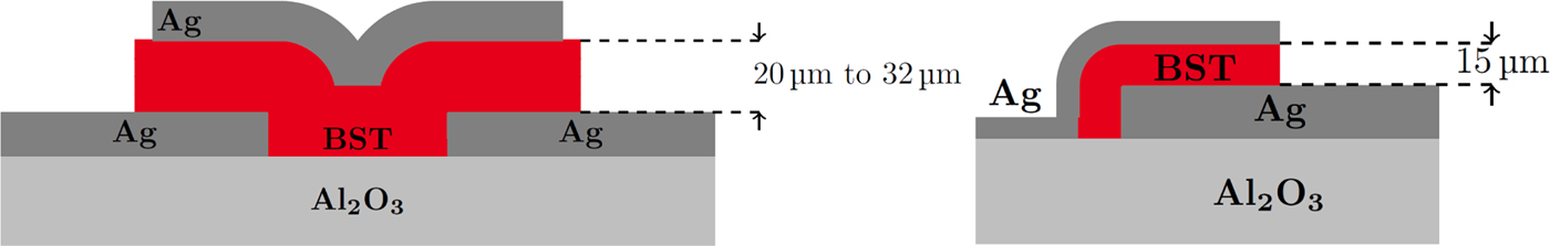
Fig. 4. Simulation model for the high-power varactor design (left) and for the acoustically optimized varactor design (right).
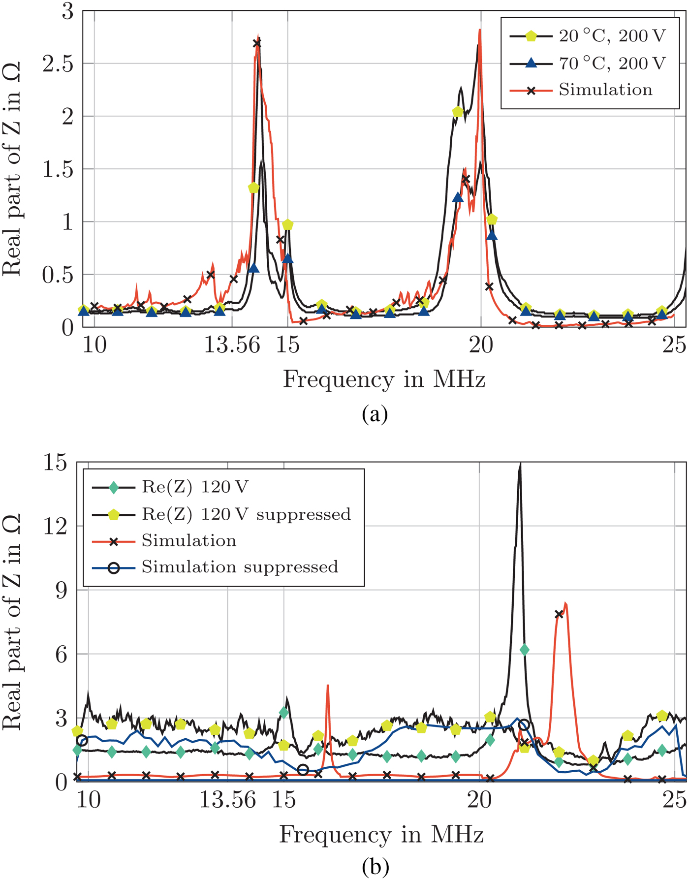
Fig. 5. Comparison between the acoustical/piezoelectric simulation and the measurement results. (a) Measured real part of the impedance versus frequency in the biased state for 20°C and 70°C as well as the acoustic simulation of the high-power optimized varactor in COMSOL. (b) Real part of the simulated and measured impedance of an acoustically optimized single varactor cell with and without acoustical suppression.
The model for the acoustically optimized varactor structure consists of a single MIM cell. In comparison with the high-power optimized structure the BST layer thickness is reduced by 25% to 15 μm and implemented as a single layer. An elastic compliance of 6 × 10⁻¹²/Pa for the BST layer is chosen in accordance with the simulation of the high-power varactor design. The simulation is repeated with an increased top electrode thickness of 100 μm to validate the narrowband acoustic suppression approach. The results of both simulations for the equivalent series resistance of the structure together with the measurement results of a single varactor cell both acoustically unsuppressed and suppressed are depicted in Fig. 5(b). Compared with the simulation results of the high-power optimized structure, depicted in Fig. 5(a), both acoustic resonances of the unsuppressed model are shifted by 2 MHz from 14 MHz and 20 MHz to 16 MHz and 22 MHz, respectively, due to the decrease in BST layer thickness. The measurement results indicate a less significant frequency shift by 1 MHz. Two possible reasons for the discrepancy of the simulation and measurement data were found: Due to the significantly lower size of the varactor, variations in thickness of the top electrode gained influence on the location of the resonances. The thickness of the top electrode was measured for 36 different varactor cells and varied in the range from 10.5 μm to 16 μm. The second reason for the discrepancy between simulation and measurement is the major impact of the elastic compliance s 33 on the location of the acoustic resonances. Simulation shows that variation of s 33 by ± 20% leads to a shift of the acoustic resonances by ∓ 200 kHz. Compared with the influence of the BST layer thickness on the position of the acoustic resonances, the impact of s 33 appears to be of similar magnitude. For most bulk materials, the elastic compliance is known. However, for thin films a major deviation has been observed, based on the film's interactions with the substrate [Reference Nix12]. Therefore, it can be assumed that a significant variation of s 33 for a BST thick film compared with the bulk material barium titanate is plausible.
The simulation of the acoustically suppressed varactor cell matches the data obtained from the measurement of the loaded varactor cells. The increased height of the top electrode flattens the resonance peaks to a width of 4 MHz and shifts the first resonance from 15 to 18 MHz. From the simulation for the loaded cell one can deduce that the acoustical behavior of the cell is no longer dominated by the elastic compliance s 33 but by the changed geometry and increased weight on the top electrode. The increased equivalent series resistance from 10 to 13.56 MHz of the suppressed simulation and measurement compared with the unsuppressed simulation and measurement indicates the presence of a resonance frequency below 10 MHz.
BST preparation and varactor processing
Cu-F codoped Ba0.6Sr0.4TiO3 is prepared in a modified sol-gel process [Reference Kohler13,Reference Zhou14]. The MIM varactor structures are processed in three steps. In the first step, the bottom RF electrodes are screen printed on an alumina substrate. For the electrodes, the conductor paste C 1076 SD (LPA 609-022) from Heraeus is chosen. It is a solderable Ag/Pt conductor paste suitable for temperatures up to 850°C. In the second step, two layers of BST thick film are screen printed on the bottom electrode and dried at 80°C. In case of the high-power optimized varactor design, two more layers of BST are printed on top. Prior investigations have shown that a minimum of four BST layers is needed to obtain a sufficient electrical strength over the large lateral dimensions of the ferroelectric layer. A total BST layer thickness of 20 μm is obtained for the high-power optimized varactor design while the acoustically optimized one features a 15 μm thick BST layer. In a final step, the top electrodes are screen printed on top of the BST layers. The varactors are co-sintered at 850°C for 10 min. The high-power varactor design is depicted in Fig. 1 together with the measurement fixture. The acoustically optimized varactor design together with the structure soldered to the FR4 measurement fixture are shown in Fig. 3. A scanning electron microscope (SEM) cross-sectional image of the printed varactor structure one is depicted in Fig. 6.
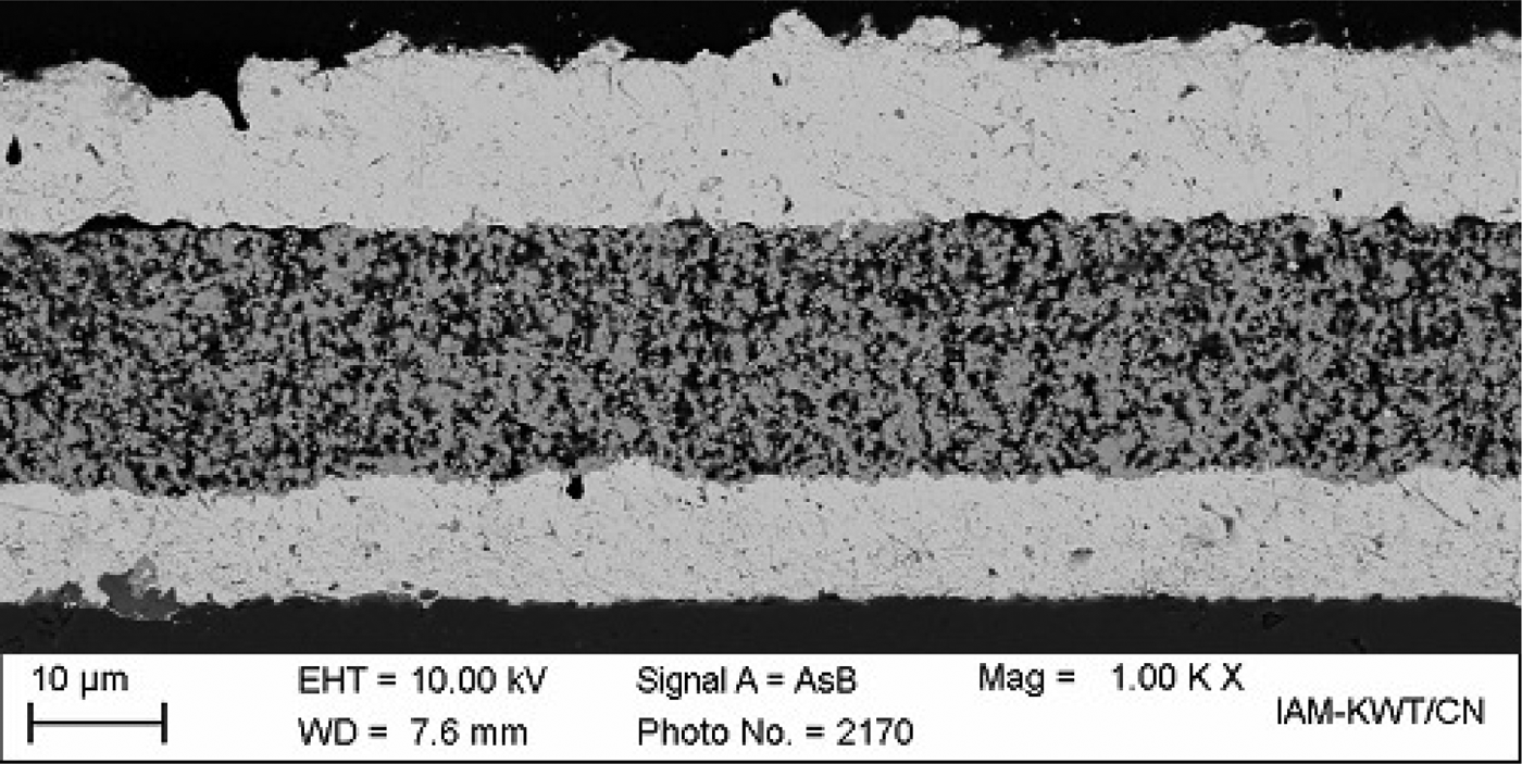
Fig. 6. Scanning electron microscope (SEM) cross-sectional image of the MIM structure.
Varactor characterization
Both varactor structures are characterized from 10 to 25 MHz with a Keysight E4991B Impedance Analyzer. For the high-power varactor structure, an additional temperature characterization is performed in the range from 20°C to 70°C. To characterize the varactor structure, it is placed in a measurement fixture depicted in Fig. 1. A fixture compensation is performed prior to the measurements, utilizing open/short structures of the designed varactor to account for the parasitic impedance of the fixture. For the temperature characterization two subminiature heating elements with a combined heating power of 18 W are applied to the back of the alumina substrate of the varactor, while it is mounted into the measurement fixture. A homogenous substrate temperature of maximum 75°C is achieved with this setup.
For the acoustically optimized varactor structure, two separate measurements are performed. First, each varactor cell is characterized using a Cascade Summit 12 K Wafer Prober with 1250 μm ground-signal probes. Subsequently, six cells per column and row are loaded with 17 mg of tin weight and remeasured. The second characterization measurement is performed on 6 × 6 exemplary interconnected varactor cells. The varactor cells are connected using a silver filled polymer. Subsequently, the structure is soldered to an FR4 PCB, which holds the resistive RF/DC decoupling network and placed in a measurement fixture.
For the high-power varactor structure the biasing voltage is adjusted in a range from 0 to 200 V. The voltage dependent tunability is calculated according to [Reference Gevorgian, Vorobiev and Lewin2]:
 $$\tau = \displaystyle{{C(0V) - C(V_{{\rm bias}})} \over {C(0V)}}.$$
The results are shown in Fig. 7. At 13.56 MHz the varactor shows a voltage dependent tunability of 37% at room temperature and 22% at 70°C. The temperature dependent change in capacitance is 31% in the unbiased state and 14% in the biased state from 20°C to 70°C. The quality factor of the varactor at room temperature in the unbiased state is 58 and increases to 93 at 70°C. However, in the biased state, the quality factor decreases at room temperature as well as at 70°C to 41 and 67, respectively. The measurement results of the quality factor show acoustic resonances of the structure at 14.2 and 19.6 MHz.
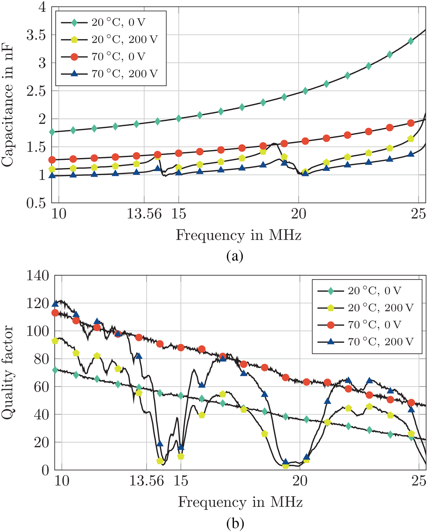
Fig. 7. Capacitance and quality factor of the high-power varactor design versus frequency. (a) Capacitance of the high-power varactor design vs. frequency in the unbiased and biased state for 20°C and 70°C. (b) Quality factor of the high-power varactor design versus frequency in the unbiased and biased state for 20°C and 70°C.
The characterization of an unloaded and loaded single varactor cell of the acoustically optimized structure is performed over a biasing voltage range from 0 to 120 V due to the reduced BST layer thickness. The results are shown in Fig. 8. The unloaded varactor cells show a maximum tunability of 31% reducing the cell capacitance from 161 to 114 pF. In biased state, the quality factor is increased by 31% from 57 to 74. The unloaded cells show acoustic resonances at 15 and 22 MHz. For the loaded varactor cells an identical capacitance and quality factor is measured in unbiased state while the biased capacitance is further reduced to 104 pF increasing the tunability to 35%. In comparison with the unloaded cells, the quality factor is tuned by 30% in the opposite direction and reduced to 43 in biased state. At the first acoustic resonance frequency of the unloaded cells however, a significantly increased quality factor of the loaded cells is measured with 58 in comparison with 28. A maximum increase of 620% in quality factor at the second acoustic resonance frequency is measured increasing the quality factor locally from 5 to 36.
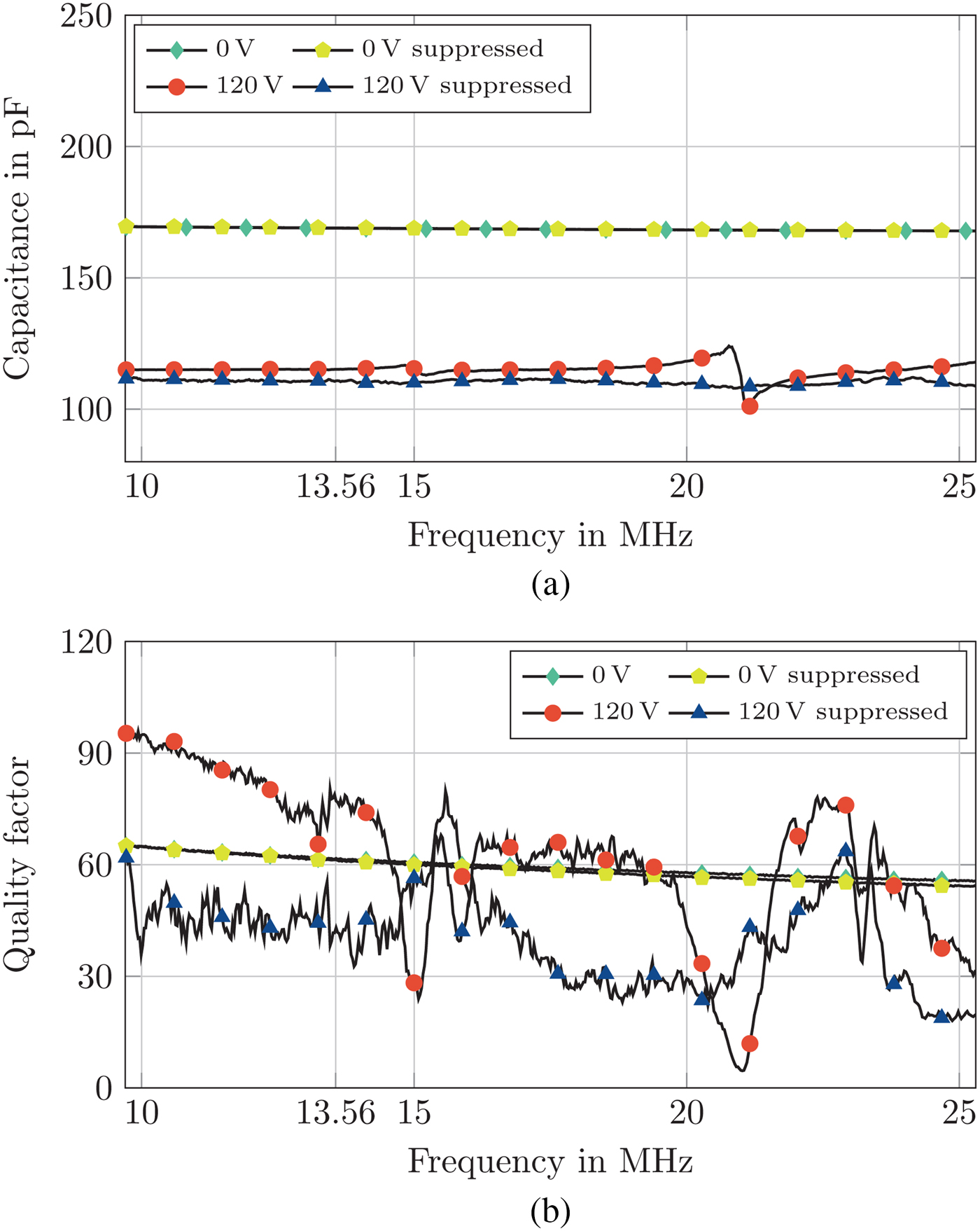
Fig. 8. Capacitance and quality factor of a single varactor cell of the acoustically optimized design versus frequency. (a) Capacitance of an unloaded and loaded varactor cell of the acoustically optimized varactor design versus frequency in the unbiased and biased state. (b) Quality factor of an unloaded and loaded varactor cell of the acoustically optimized varactor design versus frequency in the unbiased and biased state.
The results for the exemplary connected varactor matrix consisting of 6 × 6 acoustically suppressed and unsuppressed cells is shown in Fig. 9. The acoustically unsuppressed matrix shows a tunability of 41% with a biasing voltage of 0 to 200 V at 13.56 MHz reducing the capacitance from 104 to 61 pF. The quality factor in unbiased state is 60 and reduced to 57 in biased state at 13.56 MHz. In comparison with the high-power varactor design the quality factor in biased state at 13.56 MHz is significantly increased from 41 to 57 as a result of the shifted acoustic resonance at 14 MHz. For the acoustically suppressed varactor matrix the unbiased capacitance is 161 pF and shows a tunability of 47% reducing the capacitance to 79 pF at 13.56 MHz. The quality factor is reduced by 50% from 72 to 36. At 15 MHz the acoustically suppressed varactor matrix shows a quality factor of 55 compared with 22 of the unsuppressed design resulting in a significant increase of 145%. At the second acoustic resonance frequency, the increase in quality factor of the acoustically suppressed design is 400% from 4.8 to 24.
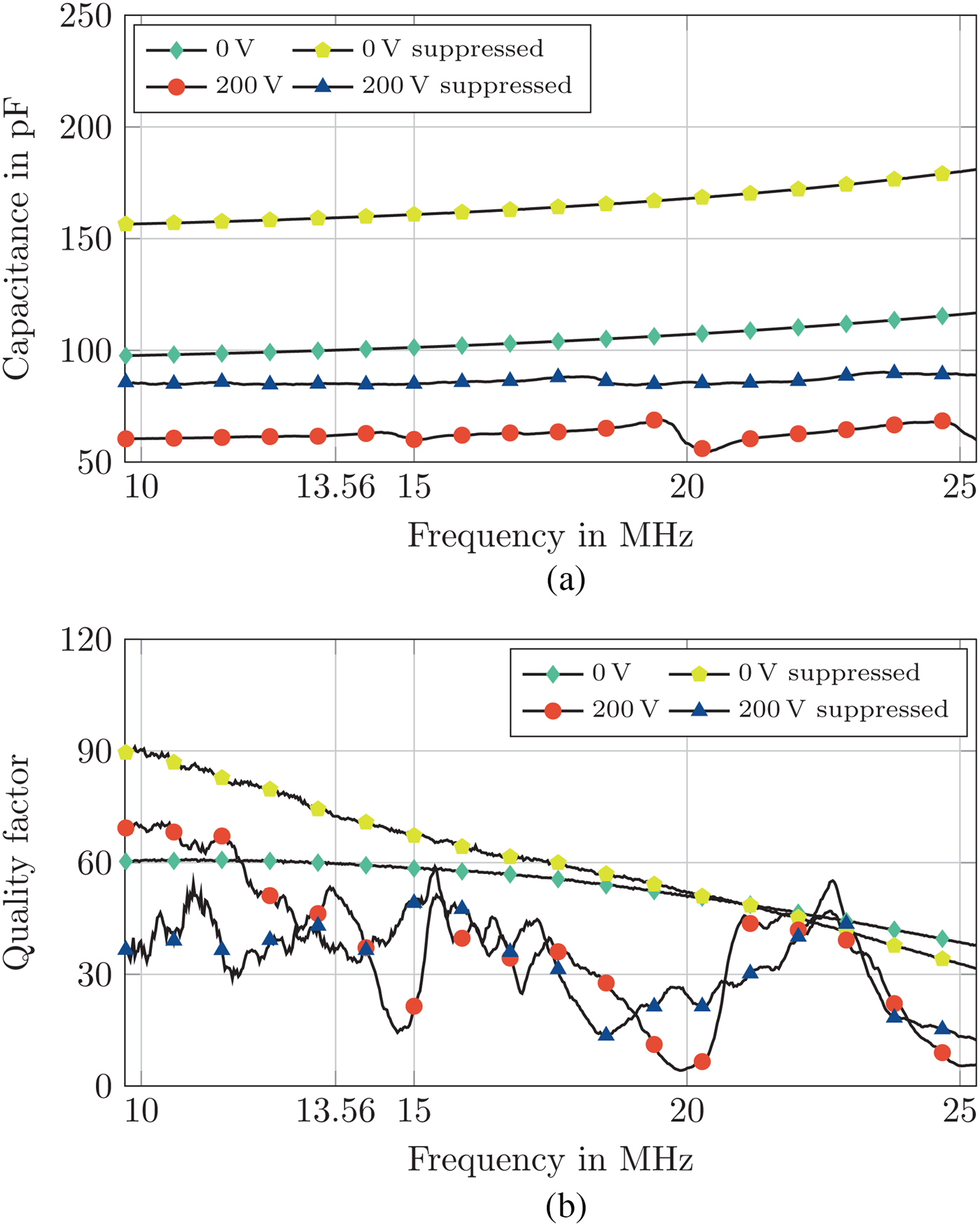
Fig. 9. Capacitance and quality factor of an exemplary varactor matrix consisting of 6 × 6 cells with and without acoustic suppression. (a) Capacitance of an exemplary varactor matrix consisting of 6 × 6 cells with and without acoustic suppression. (b) Quality factor of an exemplary varactor matrix consisting of 6 × 6 cells with and without acoustic suppression.
Conclusion
In this work two fully-printed MIM varactor designs have been presented. The first design was optimized for high-power operation and in a previous work proved full functionality in high-power matching circuits with power ratings of up to 1 kW [Reference Kienemund6]. To the best knowledge of the author, this was the first time a fully-printed component was presented capable of operation at this power level. During characterization, the high-power varactor design shows a tunability of up to 37% with 200 V of biasing voltage at room temperature. The maximum quality factor of 93 is measured at 70°C compared with 58 at room temperature. The high-power varactor shows acoustic resonances at 14.2 and 19.6 MHz which lower the quality factor at the operational frequency of 13.56 MHz in biased state. The acoustic resonances were accurately modeled utilizing a layered BST structure following the manufacturing process.
A second acoustically optimized varactor design was introduced utilizing a highly distributed capacitive matrix, thereby decreasing the thickness of the BST layer and interrupting surface acoustic resonances. Due to the modular design approach the power handling capabilities of the varactor and its unbiased capacitance are variable and can be set according to the requirements of the application. The design was validated with a piezoelectric/acoustical simulation utilizing an accurate model of a single cell of the structure. The acoustically optimized varactor cell shows a tunability of 31% with a reduced biasing voltage of 120 V. Compared with the high-power varactor the acoustically optimized varactor cell design is not affected by its first acoustic resonance and as a result an increased quality factor of 74 is measured in biased state compared with 57 in unbiased state, validating the optimization approach.
The varactor cells are utilized to demonstrate a simple narrowband acoustic suppression technique based on defined tin weights on the top electrodes of a single MIM varactor cell. The piezoelectric simulation was extended to estimate the effectiveness of the proposed suppression technique. Measurement and simulation data matched and showed a significant increase in quality factor at the acoustic resonances due to the suppression technique. A loaded varactor cell shows an increase in quality factor at the first acoustic resonance of 136% and of 620% at the second one compared with the unloaded cell. To study the acoustical behavior of an interconnected array of varactor cells a total of 36 cells were connected and characterized over a biasing voltage of 200 V. The interconnected array of unloaded varactor cells shows a capacitance tunability of 41% at 13.56 MHz. The quality factor is reduced by 5% in biased state from 60 to 57. Compared with the high-power varactor design the quality factor of the acoustically optimized design in biased state was significantly increased by 40% due to a shift of the acoustic resonance at 14.2 to 15 MHz.
To evaluate the effectiveness of the narrowband acoustic suppression technique in an array a total of 36 loaded cells were interconnected. Compared with the unloaded varactor array the quality factor of the loaded array decreases at the first acoustic resonance to 55 compared with 22. In comparison with the non-optimized high-power varactor at the first acoustic resonance frequency of 15 MHz the array of acoustically suppressed cells shows a significantly increased quality factor of 55 compared with 11 resulting in a 480% increase.
Acknowledgments
The authors would like to thank S. Schober for the sample preparation and processing.
 Daniel Kienemund received his diploma in Electrical Engineering from RWTH Aachen University in 2013. Currently he is working towards a Ph.D. in the field of tunable components for high-power radio frequency matching circuits at the Institute for Microwave Engineering and Photonics of Technische Universität Darmstadt.
 Nicole Bohn received her diploma in dental technology from Osnabrück University of Applied Sciences in 2009. Since then she is working at the Institute for Applied Materials-Ceramic Materials and Technologies of Karlsruhe Institute of Technology. Her current responsibilities include the development, fabrication and processing of tunable dielectric materials for microwave applications as well as the microstructural characterization of the specimen.
 Thomas Fink graduated with a diploma degree in Physics from Ludwig-Maximilians University in Munich in 1987, and he received a Ph.D. from Freie Universität Berlin in 1990. Subsequent affiliations include positions as research scientist at Columbia University (NY) and at Fraunhofer IAF (D) and as process engineer with ABB Semiconductors (CH). He holds a position as Senior Technology Specialist at COMET AG with focus on new variable capacitor designs for radio-frequency modules.
 Mike Abrecht obtained his Ph.D. in physics of condensed matter from the École Polytechnique Fédérale de Lausanne (EPFL), Switzerland, in 2003. In 2008 he joined the company COMET, a Swiss-based leading global provider of high-quality systems, components and services in x-ray, e-beam and RF Technologies. He is currently senior technology specialist for COMET's Plasma Control Technologies segment, where his recent activities have contributed to improved vacuum variable capacitors and other components used for industrial power delivery systems.
 Walter Bigler graduated with a diploma degree in Electrical Engineering from FH Bern in 1984. He worked over 30 years in different management positions at COMET AG, a Swiss-based leading global provider of high-quality systems, components and services in x-ray, e-beam and RF technologies. He is currently Vice President Technology in the segment Plasma Control Technologies and holds several patents as inventor and co-inventor related to Vacuum Capacitor Technologies.
 Joachim R. Binder received the diploma degree in chemistry and the Ph.D. degree from the University of Osnabrück, Germany, in 1993 and 1997, respectively. In 1997, he joined the Forschungszentrum Karlsruhe (now the Karlsruhe Institute of Technology), Germany, where he has been a group leader at the Institute of Applied Materials (IAM-KWT) since 1999. His current research is dedicated to material and process development, especially of tunable dielectrics, printed electronics and lithium ion batteries.
 Rolf Jakoby received the Dipl.-Ing. and Dr.-Ing. Degrees in electrical engineering from the University of Siegen, Germany, in 1985 and 1990, respectively. Since April 1997 he has a full professorship at TU Darmstadt, Germany. His interdisciplinary research is focused on RFID, micro- and millimeter wave detectors and sensors for various applications, and in particular on reconfigurable RF passive devices by using novel approaches with metamaterial structures, liquid crystal and ferroelectric thick/thin film technologies.
 Holger Maune received the Dipl.-Ing. and Dr.-Ing. degree in communications engineering from the Technische Universität Darmstadt, Darmstadt, Germany, in 2006 and 2011, respectively. His research focuses on reconfigurable smart radio frequency (RF) systems based on electronically tunable microwave components such as phase shifters, adaptive matching networks, tunable filters, duplexer, and multiband antennas.


