


1 Introduction
There are various solid-state pulse lasers based on Nd:glass with the output beam power of the PW level, such as the National Ignition Facility (NIF) in the United States, the MEGAJOULE (LMJ) in France, the SHENGUAN III in China, the LFEX in Japan, the Lutch in Russia, etc. The increasing of the laser pumping power leads to an increase of the inhomogeneities in the active media and the distortions of the reflective and refractive surfaces of the optical elements primarily due to heating. As a result, the wavefront of the output beam is distorted significantly. The spectrum of the distortions of the phase and of the amplitude in the high-power lasers has been observed for the wide range of the spatial frequencies  $k\approx 1\times 10^{2}{-}2.5\times 10^{-3}~\text{mm}^{-1}$ and, correspondingly, spatial lengths ranging from 0.01 to 400 mm[Reference Lawson, Aikens, English and Wolfe1, Reference Campbell, Hawley-Fedder, Stolz, Menapace, Borden, Whitman, Yu, Runkel, Riley, Feit and Hackel2]. The high-frequency components of the aberrations are usually removed with spatial filters in the optical amplifiers. The local tilts of the wavefront (wavefront aberrations), with spatial lengths ranging from 33 to 400 mm, determine the divergence and as a consequence, determine the possibility to obtain a diffraction limited focus spot. To obtain the beam intensities of ${\sim}10^{+22}~\text{W}/\text{cm}^{2}$ and more at the target–laser interaction spot, the large scale and the low-frequency wavefront aberrations have to be corrected. This is only possible with adaptive optical systems. Moreover, nowadays an adaptive optical system is mandatory in a high-power laser system.
Of course, the deformable mirror is the main element of any adaptive optical system. The parameters of the deformable mirror (size, precision of correction, resolution, laser induced damage threshold, etc.) are very important for the operation of the system. Correction efficiency depends first of all on the technology implemented on the deformable mirror. Different measurements performed in high-power lasers have shown that the real wavefront aberrations are mainly low-order ones[Reference Alexandrov, Zavalova, Kudryashov, Rukosuev, Sheldakova, Samarkin and Romanov3]. Therefore, deformable mirrors for lasers have to be adapted to correct exactly for such aberrations.
A deformable mirror with an optical surface size of  $400~\text{mm}\times 400~\text{mm}$ was developed for the NIF laser, in which 39 PMN actuators were used as active elements[Reference Zacharias, Beer, Bliss, Burkhart, Cohen, Sutton, Van Atta, Winters, Salmon, Stolz, Pigg and Arnold4]. A $220~\text{mm}\times 220~\text{mm}$ deformable mirror with 61 piezoelectric stacks with the same design has been developed for the Russian laser complex ‘Lutch’[Reference Bokalo, Garanin, Grigorovich, Jupanov, Koltygin, Kulikov, Lyakhov, Manachinsky, Mizin, Ogorodnikov, Smekalin, Smyshlyaev, Sukharev, Shanin and Schipalkin5]. Such mirrors have shown a high efficiency in correcting the wavefront of high-power pulsed lasers. However, the stroke of the piezoelectric stack actuators vary with their position below the mirror surface: their stroke at the corner of the mirror and on the external ring exceed many times the strokes of the ones located in the centre. This can reduce the reliability and the precision of the correction. For the LMJ (in France), another type of wide aperture deformable mirror was developed[Reference Grosset-Grange, Barnier, Chappuis and Hervé Cortey6]. In fact, it had a similar design as the mirror presented[Reference Zacharias, Beer, Bliss, Burkhart, Cohen, Sutton, Van Atta, Winters, Salmon, Stolz, Pigg and Arnold4], but precise positioning stepper motor actuators were used instead of piezoelectric stack actuators. Such mechanical deformable mirrors show a large amplitude of correction, a high linearity and a low hysteresis. But the considerable time it takes them to switch on and to operate (typically ${\sim}1$ sec), their large volume and their weight are the key disadvantages of this technology.
2 Bimorph deformable mirrors
Deformable mirrors based on bimorph technology are the opposite of stack actuators deformable mirrors, as they can perform a precise correction of low-order wavefront aberrations using a small number of the controlled electrodes (called bimorph actuators)[Reference Samarkin, Aleksandrov and Kudryashov7, Reference Samarkin and Kudryashov8]. A traditional semi-passive bimorph mirror consists of a comparatively thick glass substrate firmly glued to a flat thin actuator disc made of piezoelectric ceramic (Figure 1(a)). Applying an electrical signal to the electrodes placed on the piezoceramic plate causes the tension of the piezodisc due to inverse piezoelectric effect. The piezodisc expands (or shrinks, depending on the direction of polarization versus applied voltage) in the radial direction. A glued substrate prevents expansion, and this results in the bending of the reflective surface. To reproduce different types of aberrations with the help of such corrector, the outer electrode is divided into several control electrodes, which have the shape of a part of a sector. By applying a voltage to some given electrode, a local bending is caused. The rest of the surface also deforms to match the boundary conditions. This is the property of modal wavefront correctors to which bimorph mirror belongs. The size as well as the number of controlling electrodes depends upon the number, type and distribution of the aberrations to be corrected by the bimorph deformable mirror. The example of the geometry of the electrodes is given in Figure 1(b). An additional piezodisc with an all-round electrode was introduced into the design of the mirror to reproduce the general defocus and also to correct for the thermal deformation of the mirror surface. This disc is very important if you deal with high-power laser radiation introducing some heating of the mirror surface. It can also be used to compensate for the general curvature of the mirror, which appears due to the properties of the thin multilayer coating or of surface errors introduced during the manufacturing of the mirror. Figure 1(c) presents the typical response function interferograms of some electrodes of a bimorph mirror with the given pattern of electrodes. The values of the voltages are determined by the control system. The amplitude of the surface deformation achievable mainly depends on the parameters of the piezoceramic material used and on the thickness of the mirror substrate: a thinner mirror will be able to perform a higher surface deformation.
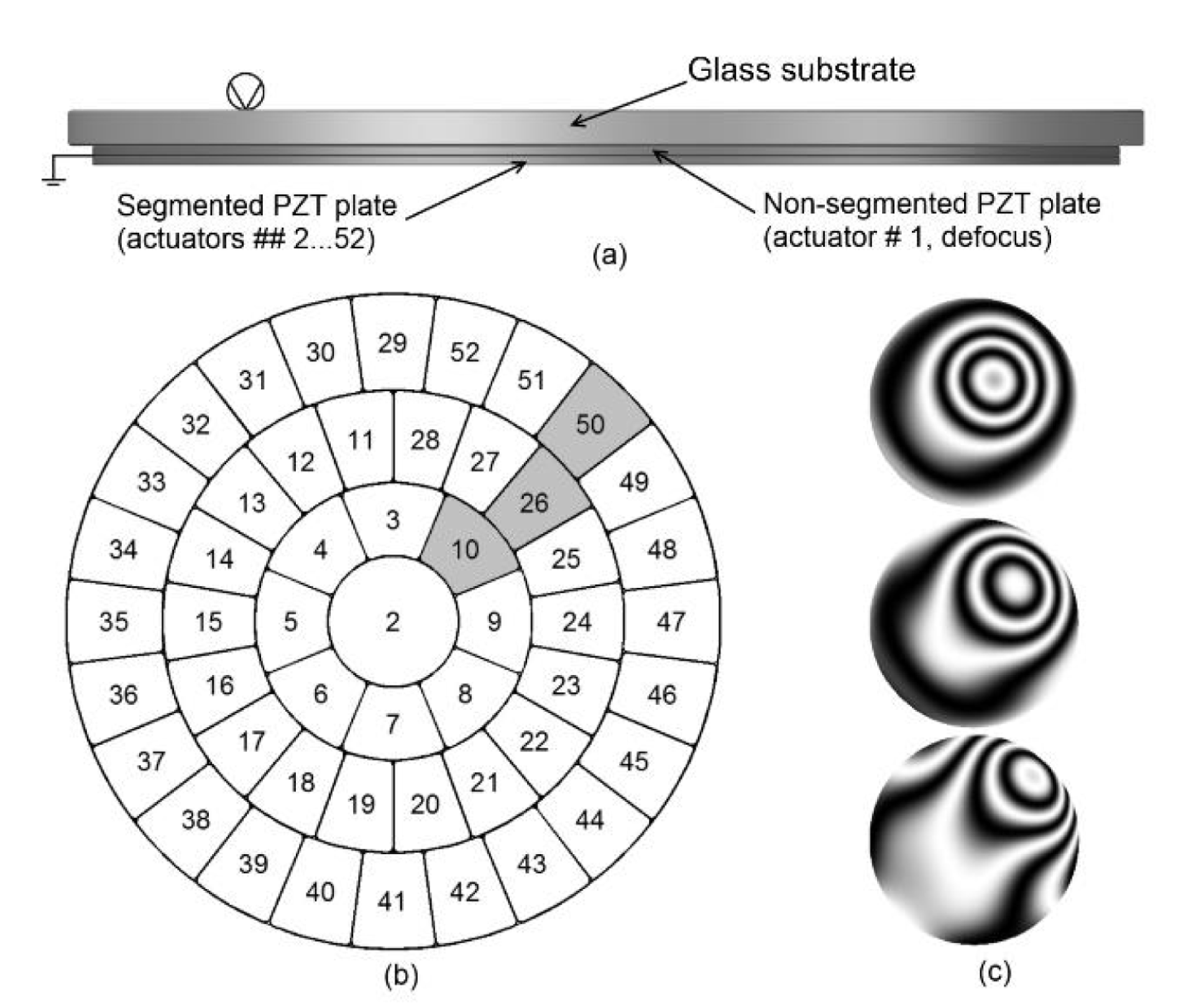
Figure 1. Design of the semi-passive bimorph mirror.
Until now, bimorph mirrors with a continuous surface diameter and a single piezoceramic disc of up to 150 mm have been developed and successfully used. Such mirrors became key mandatory elements in high-power titanium–sapphire femtosecond pulse lasers[Reference Aleksandrov, Zavalova, Kudryashov, Rukosuev and Samarkin9, Reference Sheldakova, Samarkin, Kudryashov and Rukosuev10] and PetaWatt laser systems based on Nd:glass[Reference Sueda, Jitsuno, Morio, Matsuo, Kawanaka and Miyanaga11]. However, today there is a real need for deformable mirrors of larger sizes. For example, modern lasers for the study of the laser fusion require deformable mirrors with sizes of  $400~\text{mm}\times 400~\text{mm}$ or more. The technical issue to solve to manufacture a wide aperture bimorph mirror is to attach properly the very thin and very large membrane-like bimorph mirror (the thickness to diameter ratio is $1/50$ or less) to its mount. Indeed, the main additional aberrations introduced in the mirror surface shape are located near the points of contact of the mirror with its mount. The mirror curvature is also changed by gravitation, by the variation of ambient temperature and by the heating by the laser beam. Finally, the mirror surface must withstand large laser beam energy densities (more than $30~\text{J}/\text{cm}^{2}$) and must reproduce large amplitudes ( ${\sim}100~{\rm\mu}\text{m}$) of low-order aberrations. The development of new large aperture bimorph deformable mirrors opens various areas of application for adaptive optics, for example beam correction in lasers for basic research, including laser fusion, cleaning of space orbiting debris by moving them down to the atmosphere, transfer of laser energy through turbulent media, ground and space optical communication, etc.
For mirrors with an aperture diameter of up to 200 mm, a single element piezoceramic disc glued below the full mirror area can be used. The size of the thin piezoceramic discs manufactured by the industry is now limited – unfortunately, because of the extreme fragility of the initial piezoceramic material. Therefore, larger bimorph mirrors use a mosaic structure of electrodes made with different piezoceramic plates on which metallic electrodes are deposited. The back-side view of such a bimorph mirror is presented on Figure 2, showing the electrode pattern. Four square plates of  $120~\text{mm}\times 120~\text{mm}$ and of 0.8 mm thickness were glued on the back of a $260~\text{mm}\times 260~\text{mm}$ mirror, and each of the four plates is divided into 25 small square electrodes of $24~\text{mm}\times 24~\text{mm}$. The photolithography method was used to etch by acid the metal and thus separate the electrodes electrically. The main disadvantage of this electrode structure is the presence of a global structure of a cross-like shape. The areas of the mirror above each plate are acting as an autonomous and separated mirror. As a result, mechanical tensions appear between the plates and the print through of the plates can be seen on the surface of the mirror. The print-through pattern in the laser beam is essentially influenced by the intensity distribution at the focus plane – a number of intensity peaks in the focal spot can be easily identified. It should be noted that attaching the mirror into the housing also introduces additional aberrations to the surface. The amplitude of all the aberrations, equal to the sum of the polishing imperfections, the tensions in the dielectric reflecting coating, the print-through pattern and the attachment to mounting, can be so high that it can exceed the wavefront distortions of the beam to be corrected. In that case, the full dynamic range of the control voltages will be used to compensate only for the mirror’s own aberrations, and not for the laser beam itself, which is of course not satisfying. One way to make a mirror operating in a laser with a big wavefront distortion is to simply increase the thickness of the mirror; then all aberration components will be reduced proportionally. However, the deformation stroke of the mirror will be also reduced in this case.
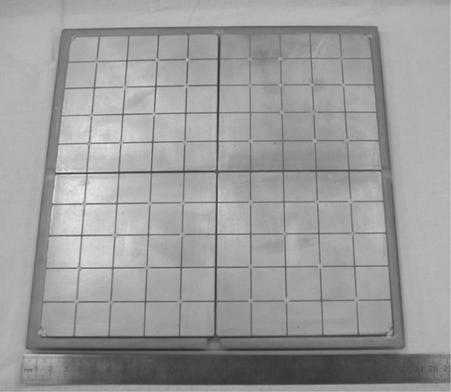
Figure 2. Electrode pattern of the bimorph mirror  $260~\text{mm}\times 260~\text{mm}$.
A bimorph deformable mirror with a relatively thick glass substrate of 8 mm, with a thickness to transverse size ratio equal to  $1/40$, has been produced. A multilayer dielectric high reflective coating optimized for the wavelength ${\it\lambda}=1.053~{\rm\mu}\text{m}$ was deposited on the mirror surface. The mirror was attached to square mounting (see Figure 3). The deformation stroke produced by the single electrodes was $6~{\rm\mu}\text{m}$. The flatness of the surface was $6~{\rm\mu}\text{m}$ (P-V) and $1.1~{\rm\mu}\text{m}$ (RMS) right after assembling it to the mounting and after a proper ‘training phase’ of the mirror, used to weaken the mechanical tensions due to the multilayer dielectric coating. The flatness was reduced to $0.14~{\rm\mu}\text{m}$ (P-V) and $0.03~{\rm\mu}\text{m}$ (RMS) after correction of the aberrations by applying the voltages to the electrodes, not exceeding 20% of the full dynamic range. Such parameters are excellent for high-power Nd:glass lasers.

Figure 3. Photo of the bimorph deformable mirror  $260~\text{mm}\times 260~\text{mm}$ attached in its mounting.
This mirror was tested in a Nd:glass laser with pulses of 400 J energy and pulses duration of 1 ns. The intensity distribution of the beam in the focal plane of the lens at the focal distance of 8 m is shown in Figure 3(a), when a flat reference mirror was installed instead of the deformable mirror, to get a reference. Here the focal spot size is 11 times larger than the diffraction limited one, according to the beam and focusing lens parameters. Then the flat reference mirror was replaced by the deformable mirror and the focal spot was recorded under the same laser beam conditions. As a result, the deformable mirror was able to correct most of the laser beam aberrations and the focal spot size was reduced to 1.3 of the diffraction limited one (Figure 4(b)).

Figure 4. Focal spot of the output laser beam: (a) before correction and (b) after correction of the wavefront; 11 and 1.3 diffraction limited sizes correspondingly.
3 Study of the wide aperture deformable mirror
In the previous chapter we described a squared  $260~\text{mm}\times 260~\text{mm}$ deformable mirror attached to its mounting. This mirror was able to improve the focus of a laser beam by a factor of 8. The only problem with this kind of mirror is that the local deformation that a single electrode can produce is rather limited – in the range of $6~{\rm\mu}\text{m}$. At the same time, increasing the size of this kind of mirror will result either in the reduction of the stroke of each electrode or in the obligation to increase the thickness to mirror size ratio (which in this case was $1/40$). As we already outlined this ratio is critical for the manufacturing and for the attachment of the mirrors in their mountings. For larger apertures, the problems with the initial mirror quality before and also after coating will even increase. This is why we have designed and manufactured a so-called combined deformable mirror, which includes both bimorph electrodes and piezostack actuators.
The clear aperture of the mirror manufactured with this technology was  $410~\text{mm}\times 468~\text{mm}$. This mirror was designed to correct the wavefront distortions of a laser beam with a size up to $400~\text{mm}\times 400~\text{mm}$ and with an angle of incidence on the mirror of $28^{\circ }$. Figure 5 shows the configuration and arrangement of the 20 piezostack actuators (SA) and 100 bimorph electrodes (BE) on the glass substrate which thickness is equal to 10 mm. The ratio of the thickness to the transverse dimension of the mirror was about $1/60$, which is supposed to induce very large initial surface aberrations. The control electrodes had the shape of a quarter of a hexagonal piezoceramic plate. The usual shape of the bimorph electrodes is round, but the real shape is not so critical in terms of response function because it is of the modal type. A rectangular distribution of the beam intensity supposes the square shape of electrodes in order to put a dense pattern of the electrodes. The hexagonal configuration of the piezoelectric plates was chosen to avoid to give a global directions to the mechanical tensions, which might cause the pattern of piezodisc to print through the mirror glass substrate, and to appear at the surface, as observed in the mirror described in Chapter 2. These piezoplates were glued to the back surface of the glass substrate on which a continuous conductive layer was deposited (this layer forms the common ground electrode for all the piezoplates). The control voltages were applied to the electrodes on the outer surfaces of the piezoelectric plates. The amplitude of the deformation of the mirror surface ranged from $-8$ to $+12~{\rm\mu}\text{m}$ for each bimorph electrode with a control voltage applied ranging from $-300$ to $+500~\text{V}$.

Figure 5. Layout and configuration of the electrodes.
The roughness of the mirror after polishing was better than 2 nm (RMS). The flatness of the surface before assembling it in its mounting was better than  $1.5~{\rm\mu}\text{m}$, it contained mostly defocus, because P-V decreased to $0.5~{\rm\mu}\text{m}$ after analytically subtracting the total curvature. The dielectric coating offered a reflection coefficient of 99.9% at the wavelength of neodymium phosphate glass laser radiation, ${\it\lambda}=1.053~{\rm\mu}\text{m}$, and the damage threshold was better than $50~\text{J}/\text{cm}^{2}$. In order to minimize the initial mirror aberrations caused by the mechanical tension after placing it into its mounting, we used the piezoelectric actuators glued on the edge of the mirror. The actuator design is a mechanical assembly including a metallic housing, a multilayer piezoceramic stack of $7~\text{mm}\times 7~\text{mm}\times 18~\text{mm}$ size (produced by PI, Germany), a spring element and screws for the mounting, the adjustment and the creation of a pre-stress (compression) of the piezostack (Figure 6).

Figure 6. Photo of the piezoelectric actuator.
The photo of the deformable mirror is shown in Figure 7. The mirror surface was analysed with a setup using a ZYGO interferometer (see optical scheme in Figure 8). A beam expanding telescope was used to increase the diameter of the diagnostic laser from 100 to 610 mm. After being reflected by the deformable mirror, the beam was reduced to 100 mm diameter and directed to the Shack–Hartmann wavefront sensor to measure the surface shape. In all our measurements, we used a ZYGO 600 mm etalon with a flatness error  ${\it\lambda}/70$ @ ${\it\lambda}=0.632~{\rm\mu}\text{m}$ (RMS) as a reference surface.

Figure 7. Combined deformable mirror: 1 – substrate with a reflective coating, 2 – actuators, 3 – metallic base.

Figure 8. Optical scheme for the analysis of the surface of the deformable mirror: 1 – 4-inch interferometer; 2–4 – folding mirrors; 5 –  $6\times$ beam expander; 6, 7 – reference surfaces; 8 – deformable mirror; 9 – beam splitter; 10 – scaling telescope; 11 – Shack–Hartmann wavefront sensor; 12 - computer with software; 13 – electronic control unit for deformable mirror.
The initial surface error after the bimorph mirror was attached to its mounting was about  $30~{\rm\mu}\text{m}$ (P-V). After a simple mechanical adjustment of the stacked actuators (with a screw driver), the peripheral flatness reached the value of $2.5~{\rm\mu}\text{m}$ (P-V). While using a standard correction procedure in a closed loop system with a Shack–Hartmann wavefront sensor[Reference Kudryashov, Samarkin, Sheldakova and Aleksandrov12], using only the stacked actuators, the aberration decreased to $1.517~{\rm\mu}\text{m}$ (P-V) (Figure 9(a)). The values of the voltages applied to the actuators are presented on the Figure 9(c) (numerically in the right-hand column and relatively by the bars below). Initially a bias voltage 50 V was applied to all actuators in order to have a possibility for bidirectional displacements of the surface. Maximal change of the voltage on the actuators was 19 V at the end of correction of the initial mirror surface. A deformable mirror with such a surface quality would initially introduce small phase aberrations in the laser beam, which need to be corrected. This additional wavefront error can be compensated by bimorph electrodes. Indeed, in the last step, when the bimorph electrodes were also activated by the closed loop the flatness obtained was equal to $0.162~{\rm\mu}\text{m}$ (P-V) and $0.033~{\rm\mu}\text{m}$ (RMS) (Figure 9(b)). The voltage values on the bimorph electrodes are also given in Figure 9(c) (numerically in the left-hand column and relatively in four bar lines in the middle). Every voltage was under 50 V that is no more than 10% of the dynamic range of the control voltage. This will save almost full control range for correction of the big amplitude aberrations of the high-power laser beam.

Figure 9. Flatness of the surface of the deformable mirror measured by wavefront sensor: (a) corrected only using the piezoelectric stack actuators ( $1.517~{\rm\mu}\text{m}$ (P-V) and $0.377~{\rm\mu}\text{m}$ (RMS)); (b) corrected using also the bimorph electrodes ( $0.162~{\rm\mu}\text{m}$ (P-V) and $0.033~{\rm\mu}\text{m}$ (RMS)); (c) map of control voltage applied both to stacked actuators and bimorph electrodes to flatten of the surface.
For a comparison, we made a direct measurement of the surface shape of the mirror with a  $600~\text{mm}$ ZYGO interferometer. This measurement showed that the flatness of the deformable mirror surface is $0.280{\it\lambda}$ (P-V) and $0.058{\it\lambda}$ (RMS) @ ${\it\lambda}=0.632~{\rm\mu}\text{m}$ (Figure 10), which pretty well fits with the measurements made with the Shack–Hartmann wavefront sensor. The resulting surface quality showed a Strehl ratio of 0.859 (Figure 11).
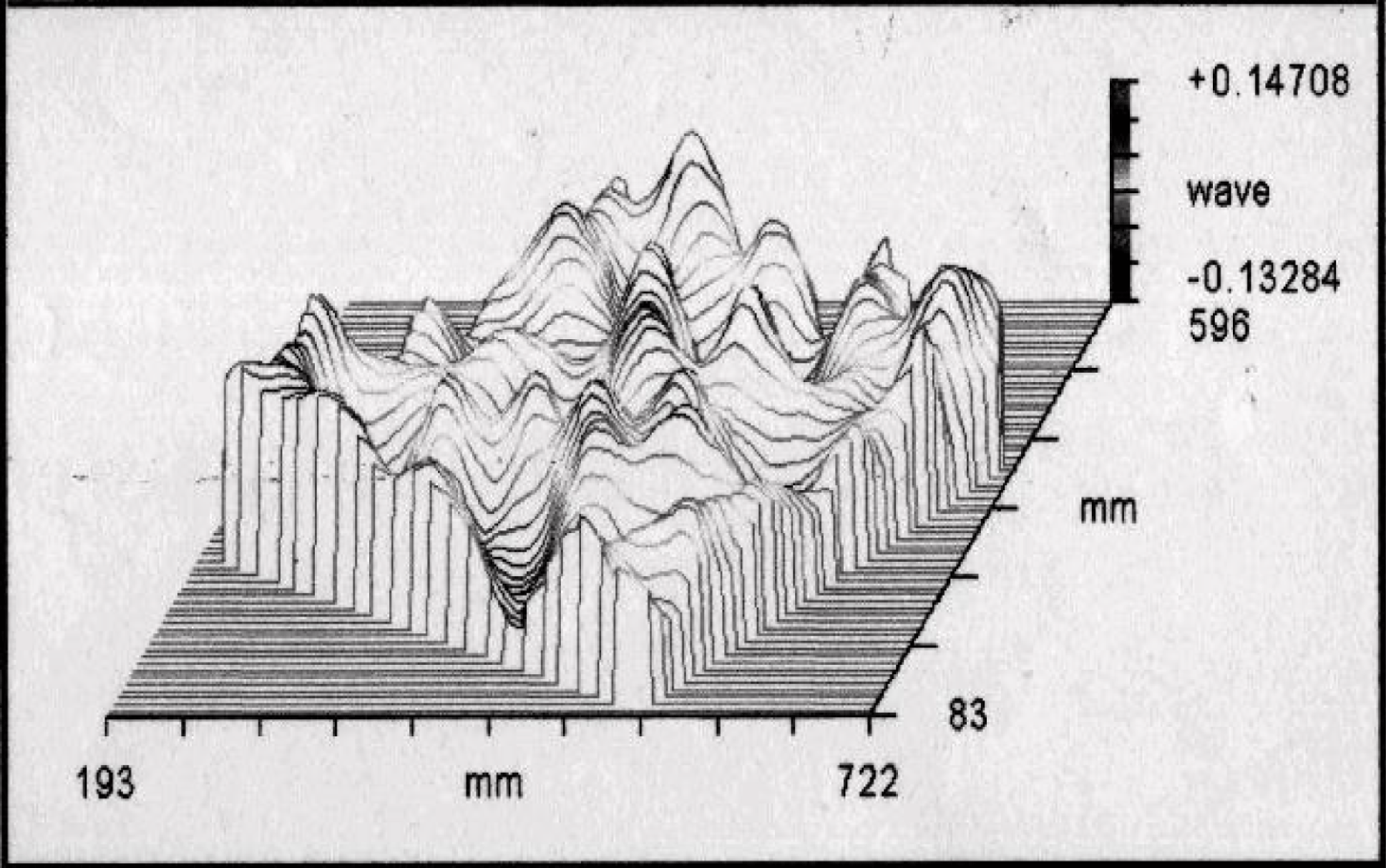
Figure 10. Flatness of the surface of the deformable mirror, corrected using also the bimorph electrodes ( $0.280{\it\lambda}$ (P-V) and $0.058{\it\lambda}$ (RMS) @ ${\it\lambda}=0.632~{\rm\mu}\text{m}$) measured with a ZYGO interferometer.

Figure 11. Point spread function of the corrected deformable mirror surface calculated by the ZYGO interferometer software – the estimated Strehl ratio is equal to 0.859.

Figure 12. Wavefront distortions of the output beam: (a) before correction and (b) after correction by means of wide aperture bimorph deformable mirror; (c) voltage map on the bimorph and stacked actuators of the mirror to correct of the wavefront distortions.
4 Wavefront correction of a high-power laser beam
Using the experimental response functions of the deformable mirror and the given wavefront distortions introduced by the optical elements of the amplifiers in the laser facility ‘Lutch’ in Russia[Reference Garanin, Golubev, Povyshev, Starikov and Shnyagin13], the ability for the mirror to correct the wavefront distortions of this laser was numerically investigated. Figure 12(a) shows the initial aberrations of the output laser beam reproduced by 36 Zernike polynomials. These aberrations were measured by a Shack–Hartmann wavefront sensor. The amplitude of the aberrations was about  $17.3~{\rm\mu}\text{m}$ (P-V) and $3.8~{\rm\mu}\text{m}$ (RMS). Based on the measured response functions of the bimorph mirror and of the stacked actuators, it was possible to calculate the voltage to be applied to the all deformable mirror actuators (bimorph and stack) in order to compensate the given wavefront aberration. Thus, for the aberration of the laser complex ‘Lutch’ presented on Figure 12(a), the numerical result of its correction with our deformable mirror was about $0.4~{\rm\mu}\text{m}$ (P-V) and $0.077~{\rm\mu}\text{m}$ (RMS) (see Figure 12(b)). The voltage map on the bimorph electrodes as well as stacked actuators (Figure 12(c)) shows that only about half of the control voltage range was used for correction. Maximal voltages were applied to the bimorph electrodes near the locations of the stacked actuators where a deformable mirror substrate is firmly fixed and correspondingly these electrodes have less stroke of the deformation. In these conditions, a Strehl ratio of better than 0.8 would be easily achieved. That should allow to focus the high-power laser beam in the diffraction limited area. We consider that this kind of deformable mirror can be used in the laser facilities of MJ level. At present our $410~\text{mm}\times 468~\text{mm}$ bimorph deformable mirror is already installed in the laser complex LFEX in Japan[Reference Azechi, Mima, Shiraga, Fujioka, Nagatomo, Johzaki, Jitsuno, Key, Kodama, Koga, Kondo, Kawanaka, Miyanaga, Murakami, Nagai, Nakai, Nakamura, Nakamura, Nakazato, Nakao, Nishihara, Nishimura, Norimatsu, Norreys, Ozaki, Pasley, Sakagami, Sakawa, Sarukura, Shigemori, Shimizu, Sunahara, Taguchi, Tanaka, Tsubakimoto, Fujimoto, Homma and Iwamoto14], where the value of the output beam power of 2 PW at 1 ps pulse duration was obtained.
5 Conclusion
The results presented in this paper demonstrate the possibility and the future applications of the bimorph mirror technology in high-power laser beam lines. Moreover, the technology we used to scale up the size of the deformable mirror opens the way, in the near future, to giant bimorph deformable mirrors of 1 m diameter or even more.


 Open access