Skip to main content Accessibility help
×
Hostname: page-component-8448b6f56d-gtxcr Total loading time: 0 Render date: 2024-04-23T16:01:36.113Z Has data issue: false hasContentIssue false

2 - An introduction to extended defects

Published online by Cambridge University Press:  10 September 2009

D. B. Holt
Affiliation:
Imperial College of Science, Technology and Medicine, London
B. G. Yacobi
Affiliation:
University of Toronto
Get access

Summary

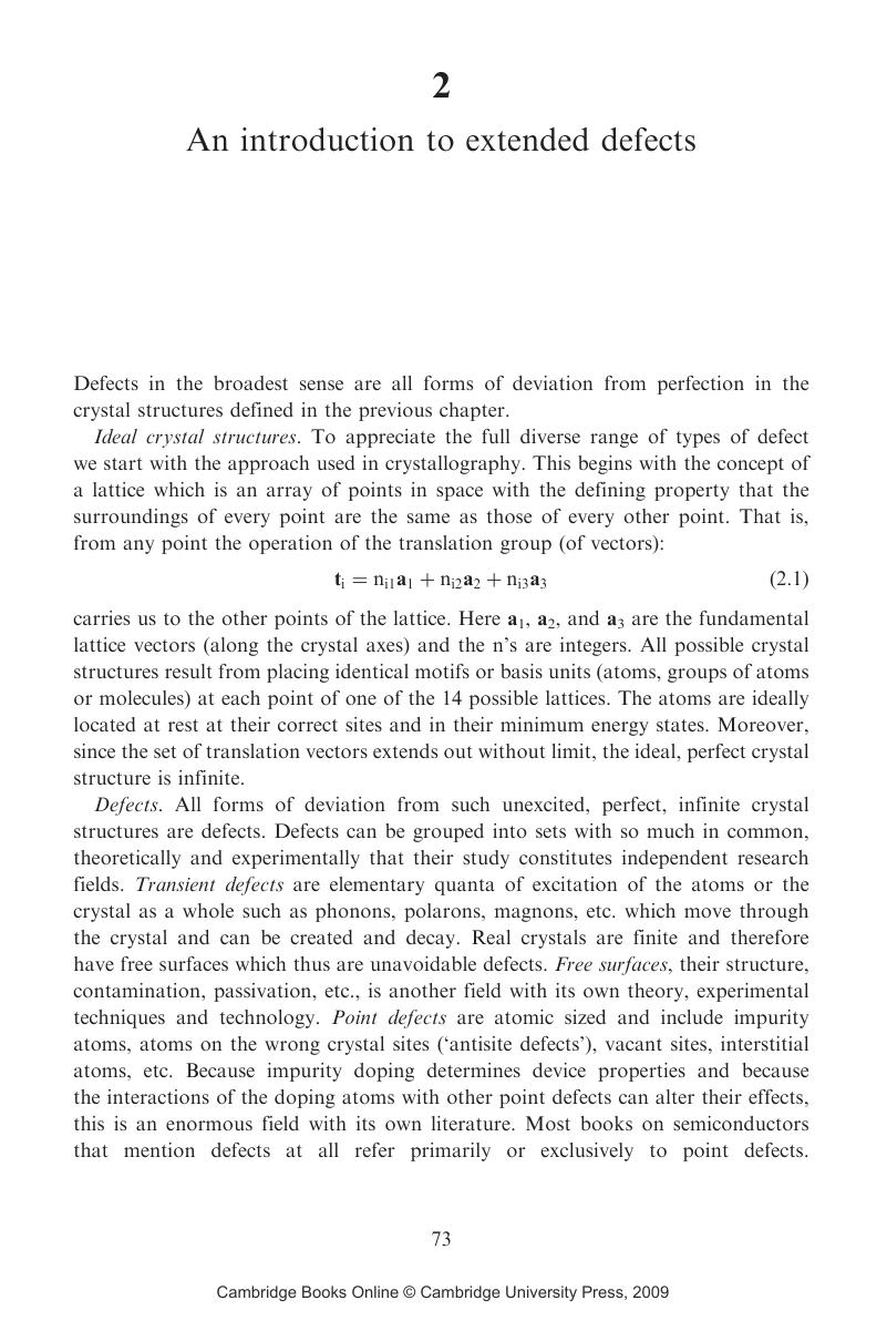
Image of the first page of this content. For PDF version, please use the ‘Save PDF’ preceeding this image.'
Type
Chapter
Information
Extended Defects in Semiconductors
Electronic Properties, Device Effects and Structures
, pp. 73 - 121
Publisher: Cambridge University Press
Print publication year: 2007

Access options

Get access to the full version of this content by using one of the access options below. (Log in options will check for institutional or personal access. Content may require purchase if you do not have access.)

References

Allen, J. W. (1959). On a new mode of deformation in indium antimonide. Philosophical Magazine, 4, 1046–54.CrossRefGoogle Scholar
Anderson, R. L. (1960). Germanium-gallium arsenide heterojuctions. IBM Journal of Research and Development, 4, 283–7.CrossRefGoogle Scholar
Anderson, R. L. (1962). Experiments on Ge-GaAs heterojunctions. Solid-State Electronics, 5, 341–51.CrossRefGoogle Scholar
Bauer, E. and Poppa, H. (1972). Recent advances in epitaxy. Thin Solid Films, 12, 167–85.CrossRefGoogle Scholar
Bauer, E. and Merwe, J. H. (1986). Structure and growth of crystalline superlattices: from monolayer to superlattice. Physical Review, B 33, 3657–71.CrossRefGoogle ScholarPubMed
Bilby, B. A. (1950). Static models of dislocations. Journal of the Institute of Metals, 76, 613–27.Google Scholar
Brantley, W. A. and Harrison, D. A. (1973). Localized plastic deformation of GaP and GaAs generated by thermocompression bonding. Journal of the Electrochemical Society, 120, 1281–4.CrossRefGoogle Scholar
Chaudhuri, A. R., Patel, J. R. and Rubin, L. G. (1962). Velocities and densities of dislocations in germanium and other semiconductor crystals. Journal of Applied Physics, 33, 2736.CrossRefGoogle Scholar
Churchman, A. T., Geach, G. A. and Winton, J. (1956). Deformation twinning in materials of the A4 (diamond) structure. Proceedings of the Royal Society, A 238, 194–203.CrossRefGoogle Scholar
Cottrell, A. H. (1953). Dislocations and Plastic Flow in Crystals. London: Oxford University Press.Google Scholar
Cottrell, A. H. and Bilby, B. A. (1949). Dislocation theory of yielding and strain ageing. Proceedings of the Physical Society, A 62, 49–62.CrossRefGoogle Scholar
Dash, W. C. (1957). The observation of dislocations in silicon. In Dislocations and Mechanical Properties of Crystals, eds. Fisher, J. C., Johnston, W. G., Thomson, R. and Vreeland, T. Jr (New York: Wiley), pp. 57–68.Google Scholar
Dash, W. C. (1958). The growth of silicon crystals free from dislocations. In Growth and Perfection of Crystals, eds. Doremus, R. H., Roberts, B. W. and Turnbull, D. (New York: Wiley), pp. 361–85.Google Scholar
Dash, W. C. (1960). Gold-induced climb of dislocations in silicon. Journal of Applied Physics, 31, 2275–83.CrossRefGoogle Scholar
Davies, G. J. and Williams, R. H. (eds.) (1994). Semiconductor Growth, Surfaces and Interfaces. London: Chapman & Hall.Google Scholar
Frank, F. C. (1949). Answer by Frank in discussion of a paper by N. F. Mott that introduced what became known as Frank's rule. Physica, 15, 131–3.Google Scholar
Frank, F. C. and Merwe, J. H. (1949a). One-dimensional dislocations. I Static theory. Proceedings of the Royal Society, A 198, 205–16.CrossRefGoogle Scholar
Frank, F. C. and Merwe, J. H. (1949b). One-dimensional dislocations. II Misfitting monolayers and oriented overgrowth. Proceedings of the Royal Society, A 198, 216–25.CrossRefGoogle Scholar
Frank, F. C. and Read, W. T. (1950). Multiplication processes for slow moving dislocations. Physical Review, 79, 722–3.CrossRefGoogle Scholar
Friedel, G. (1926). Lecons de Cristallographie (Paris: Berger Levrault), pp. 250–2.Google Scholar
Gilman, J. J. (1969). Micromechanics of Flow in Solids. New York: McGraw-Hill.Google Scholar
Haasen, P. and Alexander, H. (1968). Dislocations and plastic flow in the diamond structure. Solis State Physics, 22, 27–158.Google Scholar
Hah, S. R. and Fischer, T. E. (1998). Tribochemical polishing of silicon nitride. Journal of the Electrochemical Society, 145, 1708–14.CrossRefGoogle Scholar
Heydenreich, J. (1985). Electron microscopical characterization of electronic materials. In Crystal Growth of Electronic Materials, ed. Kaldis, E. (Amsterdam: North-Holland), pp. 325–41.Google Scholar
Hill, M. J. and Rowcliffe, D. J. (1974). Deformation of silicon at low temperatures. Journal of Materials Science, 9, 1569–76.CrossRefGoogle Scholar
Hirsch, P. B. (1985). Dislocations in semiconductors. Materials Science and Technology, 1, 666–77.CrossRefGoogle Scholar
Hirth, J. P. and Lothe, J. (1968). Theory of Dislocations. New York: McGraw-Hill.Google Scholar
Holt, D. B. (1966). Misfit dislocations in semiconductors. Journal of Physics and Chemistry of Solids, 27, 1053–67.CrossRefGoogle Scholar
Holt, D. B. (1984). Polarity reversal and symmetry in semiconducting compounds with the sphalerite and wurtzite structures. Journal of Materials Science, 19, 439–46.CrossRefGoogle Scholar
Hornstra, J. (1958). Dislocations in the diamond lattice. Phys. Chem. Solids, 5, 129–41.CrossRefGoogle Scholar
Hornstra, J. (1959). Models of grain boundaries in the diamond lattice I. Tilt about 〈110〉. Physica, 25, 409–22.CrossRefGoogle Scholar
Hornstra, J. (1960). Models of grain boundaries in the diamond lattice. II. Tilt about 〈001〉 and theory. Physica, 26, 198–208.CrossRefGoogle Scholar
Hull, D. and Bacon, D. J. (1984). Introduction to Dislocations. 3rd edn. Oxford: Pergamon.Google Scholar
Kabler, M. N. (1963). Dislocation mobility in germanium. Physical Review, 131, 54.CrossRefGoogle Scholar
Mahajan, S. and Sree Harsha, K. S. (1999). Principles of Growth and Processing of Semiconductors. New York: McGraw-Hill.Google Scholar
Matthews, J. W. (1975). Coherent interfaces and misfit dislocations. In Epitaxial Growth Part B, ed. Matthews, J. W. (New York: Academic Press), pp. 559–609.Google Scholar
Matthews, J. W. (1979). Misfit dislocations. In Dislocations in Solids, Vol. 2, ed. Nabarro, F. R. N. (Amsterdam: North-Holland), pp. 461–545.Google Scholar
Muratov, V. A. and Fischer, T. E. (2000). Tribochemical polishing. Annual Review of Materials Science, 30, 27–51.CrossRefGoogle Scholar
Nabarro, F. R. N., Holt, D. B. and Basinski, Z. S. (1964). Plasticity of pure single crystals. Advances in Physics, 13, 193.CrossRefGoogle Scholar
Nolder, R. and Cadoff, I. (1965). Heteroepitaxial silicon–aluminium oxide interface. Part II – orientation relations of single-crystal silicon on alpha aluminium oxide. Transactions of the Metallurgical Society of AIME, 233, 549–56.Google Scholar
Oldham, W. G. and Milnes, A. G. (1964). Interface states in semiconductor heterojunctions. Solis State Electronics, 7, 153–65.CrossRefGoogle Scholar
Ossipiyan, Yu. A., Petrenko, V. F., Zaretskii, A. V. and Whitworth, R. W. (1986). Properties of II-VI semiconductors associated with moving dislocations. Advances in Physics, 35, 115–88.CrossRefGoogle Scholar
Pashley, D. W. (1956). The study of epitaxy in thin surface films. Advances in Physics, 5, 173–240 (plus plates 1 to 10).CrossRefGoogle Scholar
Pashley, D. W. (1991). The epitaxy of metals. In Processing of Metals and Alloys, ed. Cahn, R. W.. Materials Science and Technology: A Comprehensive Treatment, Vol. 15 (Weinheim: VCH), pp. 289–328.Google Scholar
Peierls, R. E. (1940). The size of a dislocation. Proceedings of the Physical Society of London, 52, 34–7.CrossRefGoogle Scholar
Pirouz, P. (1987). Deformation mode in silicon, slip or twinning?Scripta Metallurgica, 21, 1463–8.CrossRefGoogle Scholar
Pirouz, P. and Ning, X. J. (1995). Partial dislocations in semiconductors: structure, properties and their role in strain relaxation. In Microscopy of Semiconducting Materials 1995. Conf. Series No. 146 (Bristol: Inst. Phys.), pp. 69–77.Google Scholar
Pirouz, P., Samant, A. V., Hong, M. H., Moulin, A. and Kubin, L. P. (1999). On deformation and fracture of semiconductors. In Microscopy of Semiconducting Materials 1999. Conf. Series No. 164 (Bristol: Inst. Phys.), pp. 61–6.Google Scholar
Read, W. T. (1953). Dislocations in Crystals. New York: McGraw-Hill.Google Scholar
Royer, L. (1928). Recherches experimentales sur l'epitaxie ou orientation mutuele de cristaux d'especes differentes. Bulletin of the French Society of Mineralogy, 51, 7–159.Google Scholar
Schafer, S. (1967). Messung von versetzungsgeschwindigkeiten in germanium. Physica Status Solidi, 19, 297.CrossRefGoogle Scholar
Seeger, A. (1957). The origin of the small angle scattering of x-rays in plastically deformed metals. Acta Metallurgica, 5, 24–8.CrossRefGoogle Scholar
Sharma, B. L. and Purohit, R. K. (1974). Semiconductor Heterojunctions. Oxford: Pergamon Press.Google Scholar
Shockley, W. (1953). Dislocations and edge states in the diamond crystal structure. Physical Review, 91, 228.Google Scholar
Shockley, W. and Read, W. T. (1949). Quantitative predictions from dislocation models of crystal grain boundaries. Physical Review, 75, 692.CrossRefGoogle Scholar
Shockley, W. and Read, W. T. (1950). Dislocation models of crystal grain boundaries. Physical Review, 78, 275–89.Google Scholar
Stickler, R. and Booker, G. R. (1963). Surface damage on abraded silicon specimens. Philosophical Magazine, 8, 859–76.CrossRefGoogle Scholar
Thompson, N. (1953). Dislocation nodes in face-centred cubic lattices. Proceedings of the Physical Society of London, B66, 481–92.CrossRefGoogle Scholar
Vogel, F. L., Pfann, W. G., Corey, H. E. and Thomas, E. E. (1953). Observations of dislocations in lineage boundaries in germanium. Physical Review, 90, 489–90.CrossRefGoogle Scholar
Wessel, K. and Alexander, H. (1977). On the mobility of partial dislocations. Philosophical Magazine, 35, 1523–36.CrossRefGoogle Scholar

Save book to Kindle

To save this book to your Kindle, first ensure coreplatform@cambridge.org is added to your Approved Personal Document E-mail List under your Personal Document Settings on the Manage Your Content and Devices page of your Amazon account. Then enter the ‘name’ part of your Kindle email address below. Find out more about saving to your Kindle.

Note you can select to save to either the @free.kindle.com or @kindle.com variations. ‘@free.kindle.com’ emails are free but can only be saved to your device when it is connected to wi-fi. ‘@kindle.com’ emails can be delivered even when you are not connected to wi-fi, but note that service fees apply.

Find out more about the Kindle Personal Document Service.

Available formats
×

Save book to Dropbox

To save content items to your account, please confirm that you agree to abide by our usage policies. If this is the first time you use this feature, you will be asked to authorise Cambridge Core to connect with your account. Find out more about saving content to Dropbox.

Available formats
×

Save book to Google Drive

To save content items to your account, please confirm that you agree to abide by our usage policies. If this is the first time you use this feature, you will be asked to authorise Cambridge Core to connect with your account. Find out more about saving content to Google Drive.

Available formats
×